


- News
25 April 2019
Gallium-doped zinc oxide transparent conductor for gallium nitride LEDs
Gwangju Institute of Science and Technology in South Korea has used a gallium-doped zinc oxide (ZnO) transparent conducting layer (TCL) to enhance the performance of indium gallium nitride (InGaN) light-emitting diodes (LEDs) [Sang-Jo Kim et al, Optics Express, vol27, pA458, 2019]. The researchers found that the ZnO TCL reduced strain in the InGaN light-emitting material, increasing light output power and reducing forward voltage, compared with a device using indium tin oxide (ITO) as a TCL.
Another advantage of ZnO over ITO is cost: indium is an expensive rare element. Further concerns about ITO include thermal instability – particularly important in high-power LEDs where junction temperatures tend to be higher. The researchers comment: “Compared with ITO, ZnO boasts the advantages of higher transmittance, lower resistivity, improved temperature stability, lower cost and non-toxicity”
Increasing light output power and reducing forward voltages are key factors in improving the efficiency of LEDs. InGaN LEDs are widely deployed in liquid-crystal display backlight units, full-color displays, automotive lighting, and general illumination.
C-plane sapphire served as substrate for the metal-organic chemical vapor deposition (MOCVD) LED structure (Figure 1). The InGaN/GaN quantum well active region was designed for a 460nm emission wavelength.
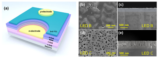
Figure 1: (a) Schematic of LED with Ga-doped ZnO TCL. Top-view and cross-sectional scanning electron microscope images of ZnO TCLs with thicknesses of: (b), (c) 180nm (LED B) and (d), (e) 500nm (LED C).
Fabrication began with mesa etching to expose the buried n-GaN contact layer. The Ga-doped ZnO TCL was grown by 650°C MOCVD on the p-GaN, using diethylzinc, oxygen and triethylgallium. Annealing at 700°C removed ZnGa2O4 interface inclusions that increase series resistance. The structure was etched with hydrochloric acid solution to clear the pad areas of ZnO. Contact electrodes for both and p- and n-sides of the device consisted of titanium/gold.
Raman spectroscopy indicated that increasingly thick ZnO layers relaxed the compressive strain of the active layers. The estimates for biaxial strain from the Raman-shift measurements were −6.76%, −5.67% and −4.57%, for ZnO layers of 0nm (LED A with 180nm ITO TCL), 180nm (B) and 500nm (C), respectively. Relaxing the compressive strain blue-shifted the emitted radiation wavelength peak in photoluminescence (PL) experiments from 464.1nm down to 456.9nm. At the same time the estimated internal quantum efficiency (IQE) increased by up to 16.5%.
The researchers comment: “The blue-shift of PL peak and enhanced IQE are attributed to the increased radiative recombination rates caused by the increased overlap of electron and hole wavefunctions owing to the reduced quantum-confined Stark effect (QCSE) in the active region of LED B and C compared with that of LED A”.
The QCSE is an energy-level shift arising from the induced electric field in III-nitride structures due to charge polarization of the chemical bonds, which is strongly affected by lattice strain. The electric field also inhibits recombination of the electrons and hole by pulling them apart.
Under electrical bias, the peak wavelengths of the LEDs converged to between 445nm and 454nm at 100mA injection. At 10mA injection, LED A’s peak was at 460.3nm, and that of LED C at 455.7nm. The convergence of LED A with a blue-shift of 6.13nm from 10mA injection was due to injected carriers screening the piezoelectric field and filling up the conduction band. LEDs B and C registered far smaller shifts of 1.99nm and 1.93nm, respectively. The smaller shift in B and C reflected the reduced piezoelectric fields due to less strain.
The light output power at 100mA was increased for LEDs B and C by 26.9% and 30.9%, respectively, over LED A’s performance (Figure 2). The improvement was attributed to increased radiative recombination due to reduced strain, and enhanced light extraction from the higher refractive index of ZnO compared with ITO. The output power was maintained in repeated experiments over a five-day period.
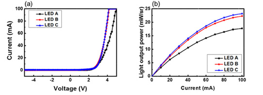
Figure 2: (a) Current-voltage characteristics and (b) optical output power of LEDs A, B and C.
The electrical performance gave the forward voltage at 20mA as 3.42V, 3.23V and 3.28V for LEDs A-C in order. The lower voltages for B and C indicate reduced power consumption. The researchers attribute the lower voltages to lower resistance of the ZnO TCL, resulting from higher carrier concentration and mobility.
While the TCL of LED C had a higher carrier concentration (2.87x10²⁰/cm3) than LED B (2.31x10¹⁹/cm3), the mobility order was reversed – 32.8cm2/V-s for LED B and 23.7cm2/V-s for C. The carrier density and mobility for LED A were 1.64x10¹⁹/cm3 and 6.07cm2/V-s. The resistivity of the TCL materials for A-C were, in order, 3.1x10⁻⁴Ω-cm, 5.3x10⁻⁴Ω-cm and 5.2x10⁻⁴Ω-cm.
Gallium-doped ZnO InGaN LEDs ZnO InGaN
https://doi.org/10.1364/OE.27.00A458
The author Mike Cooke is a freelance technology journalist who has worked in the semiconductor and advanced technology sectors since 1997.


