


- News
3 April 2019
Curved mirror reduces threshold of gallium indium nitride vertical laser
Japan’s Sony Corp claims the lowest threshold current recorded for a gallium indium nitride (GaInN)-based blue vertical-cavity surface-emitting laser (VCSEL) [Tatsushi Hamaguchi et al, Appl. Phys. Express vol12, p044004, 2019].
The researchers say that their achievement was enabled by lateral optical confinement by incorporation of a curved mirror in the vertical cavity structure. The team adds: “According to classical Gaussian optics, the current aperture can theoretically be as small as the diffraction limit, i.e. the order of the light wavelength, which suggests that further miniaturization and reduction of GaN-based VCSELs with curved mirrors could be achieved.”
The researchers see applications arising from the low threshold current, arraying capabilities and high-frequency operation. More concretely, such features are desired for optical storage, laser printers, projectors, displays, solid-state lighting, optical communications and biosensors. The low threshold was enabled by reducing the current aperture to 3μm. The lateral confinement of the curved mirror reduced the beam waist to 1.3μm on the planar mirror.
The epitaxial material was grown on a {0001} GaN substrate. The active light-generating region was a GaInN quantum well structure sandwiched between n- and p-type GaN contacts.
Fabrication on the top-side of the wafer added layers of transparent indium tin oxide (ITO) conductor and a distributed Bragg reflector (DBR) constructed from 11.5 tantalum pentoxide/silicon dioxide (Ta2O5/SiO2) pairs.
Boron (B++) implantation restricted current flow to a 3μm-diameter aperture. The metal electrodes on the ITO and n-GaN consisted of titanium/platinum/gold.
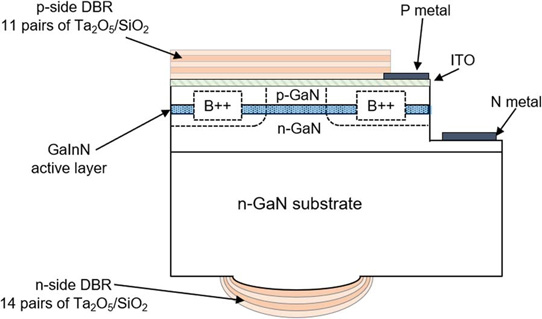
Figure 1: Schematic of VCSEL with curved back-mirror.
The back-side fabrication consisted of substrate thinning to less than 50μm thick, followed by reactive ion etch to form a curved mirror structure (Figure 2). The device (Figure 1) was completed by vacuum deposition of 14 Ta2O5/SiO2 pairs to form a curved DBR back-side reflector.
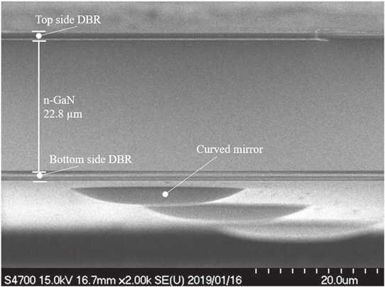
Figure 2: Cross-sectional scanning electron micrograph of device.
The threshold for continuous-wave lasing came at 0.25mA current (3.5kA/cm2 density). This value was lower than the researchers’ previous achievement of 40mA in a pulsed injection set up. Normally, pulsed injection leads to lower thresholds than continuous-wave operation due to self-heating effects in the latter case.
The improvement in the latest device is variously attributed to factors such as “reduction in the ITO layer thickness and number of quantum wells”. The group’s previous device had four wells – this was reduced to three in the latest VCSEL. The ITO thickness was decreased from 30nm to 20nm.
The dominant peak had a blue wavelength of 445.3nm (λ). The peak width was at the 0.1nm order of resolution of the spectral analyzer. Other peaks came at 1.27nm separation in wavelength, consistent with a 27μm cavity length based on a refractive index of 2.45 (n) with -0.001/nm variation in wavelength (dn/dλ).
https://doi.org/10.7567/1882-0786/ab03eb
The author Mike Cooke is a freelance technology journalist who has worked in the semiconductor and advanced technology sectors since 1997.


