


- News
11 April 2019
First demonstration of RF N-polar GaN metal-insulator-semiconductor HEMT
University of California Santa Barbara (UCSB) in the USA has reported the first radio frequency (RF) nitrogen-polar gallium nitride-on-gallium nitride (GaN-on-GaN) metal-insulator-semiconductor high-electron-mobility transistor (MISHEMT) [Shubhra S Pasayat et al, Semicond. Sci. Technol., vol34, p045009, 2019]. Using GaN substrates enabled the dislocation density to be reduced, minimizing carrier scattering at the low charge densities typical for transistors used in AB-mode amplification.
The researchers are keen to develop solutions for millimeter-wave RF applications in sensing and communication that variously employ frequency bands in atmospheric absorption and transmission windows. The N-polar orientation reverses the usual Ga-polar structure. In particular, the channel layer of mobile charges is induced by a back-barrier rather than a top barrier. N-polar devices tend to have higher power output, but reduced efficiency.
AB-mode amplification biases transistors towards pinch-off when channel carrier densities are low. AB operation reduces dissipation losses and higher efficiency is obtained when the bias is towards the B-mode rather than A-mode end of the trade-off, so-called ‘deep’ AB biasing. In N-polar devices, such biasing suffers from a degradation in electron mobility that apparently arises from scattering off the back-barrier. By contrast, in Ga-polar devices deep AB biasing pushes the electrons away from the top barrier interface.
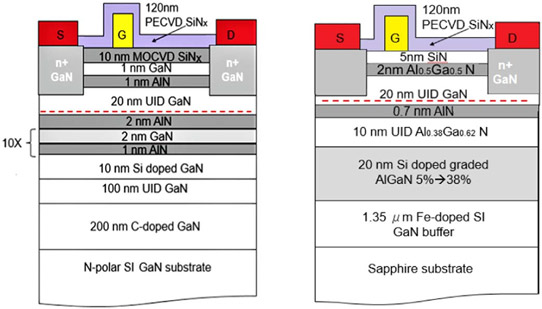
Figure 1: (a) N-polar HEMT device PAMBE structure and fabrication cross-section. (b) Conventional MOCVD grown N-polar GaN HEMT.
The epitaxial structure for the device (FIgure 1) was grown by plasma-assisted molecular beam epitaxy (PAMBE) on on-axis semi-insulating bulk GaN. The carbon (C) doping of the 200nm GaN buffer continued the semi-insulating character of the substrate. The back-barrier was prepared with 100nm of unintentionally doped (UID) material, followed by 10nm of n-GaN, which was used to control the position of the Fermi level in the overlying structure.
The barrier itself consisted of a 10-period super-lattice of 1nm/2nm AlN/GaN, and capped with 2nm of AlN. This structure induced a two-dimensional electron gas in the 20nm UID GaN channel layer. The 2nm AlN layer reduced barrier interface scattering.
The researchers explain why they used the super-lattice structure: “Due to a lag between the rate of aluminium cell temperature change in PAMBE and the optimum growth rate for N-polar AlGaN/GaN structure, an interruption-free linearly graded AlGaN growth was not possible.”
The epitaxial material was completed with 1nm/1nm AlN/GaN. The super-lattice was designed to have an effective 33% Al content, while the cap had an effective 50% Al content. The channel mobility was 800cm2/V-s, about 60% higher than for a GaN-on-sapphire structure.
Further PAMBE was used to selectively deposit n+-GaN contacts through a silicon dioxide mask. Further transistor fabrication included metal-organic chemical vapor deposition (MOCVD) of silicon nitride gate dielectric, reactive-ion mesa etching, source/drain contact titanium/gold ohmic metal electrode deposition, and gate and contact pad deposition of titanium/gold. A 120nm plasma-enhanced chemical vapor deposition (PECVD) silicon nitride layer provided passivation.
The gate had two wings of 25μm width (2x25μm) and 0.75μm length. The gate was placed at 0.5μm distance from the source contact. The source-drain distance was 5μm. With the gate at 0V relative to the source (VGS), the on-resistance was ~2Ω-mm. The maximum drain current was 1.1A/mm at almost 5V VDS. The peak transconductance was ~200mS/mm with the gate at -4.2V and the drain at 4V.
The current was slightly higher under pulsed operation, suggesting a self-heating effect. In many GaN-based transistors there is significant current collapse/dispersion where the charge flow is lower under pulsed operation. There was no such dispersion/collapse observed with the UCSB device.
Frequency cut-offs (Figure 2) were determined with the device biased at -4.5V VGS and 8V VDS: 14.6GHz for maximum oscillation/power gain (fmax) and 8.9GHz for current gain (ft). The biasing produced a drain current of 0.598A/mm. The cut-off values were determined without pad de-embedding.
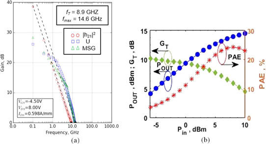
Figure 2: (a) Small-signal gain data for simultaneous peak ft and fmax and (b) 4GHz load-pull power sweep.
Load-pull measurements at 4GHz were performed to assess large-signal performance. Class AB biasing was used with the drain current at 270mA/mm, about a quarter of the maximum (-6V VGS, 5V VDQ,Q). This optimized power-added efficiency (PAE) at 4GHz in its trade-off with gain. The output power density reached 0.56W/mm. The maximum PAE was 24%.
The researchers hope to achieve deep AB biasing in future scaled and optimized devices. For example, the gate-to-drain breakdown voltage of ~15V needs to be increased to enable increased gain and PAE at low charge density.
RF N-polar GaN HEMT MISHEMT GaN MOCVD
https://doi.org/10.1088/1361-6641/ab0761
The author Mike Cooke is a freelance technology journalist who has worked in the semiconductor and advanced technology sectors since 1997.


