


- News
16 August 2019
Thermal atomic layer etching of III-arsenide semiconductors
Massachusetts Institute of Technology and University of Colorado in the USA have been exploring the potential of thermal atomic layer etching (ALE) of III-arsenide compound semiconductor materials with a view to the production of electronic devices such as fin field-effect transistors (finFETs) [Wenjie Lu et al, Nano Letters, published online 28 June 2019].
Thermal ALE is like thermal atomic layer deposition (ALD) in reverse. The first report, in 2015, was for a process that etched aluminium oxide (Al2O3).
The researchers used a viscous-flow, hot-wall ALD reactor to perform the ALE. The process was developed on templates with 70nm indium gallium arsenide (In0.53Ga0.47As) on a 300nm indium aluminium arsenide (In0.52Al0.48As) buffer. The substrate for the molecular beam epitaxy (MBE) of the templates was semi-insulating indium phosphide (InP).
The team studied three ALE recipes: hydrogen fluoride (HF) and trimethyl-aluminium (Al(CH3)3, TMA), with and without ozone; and hydrogen fluoride and dimethyl-aluminium chloride (AlCl(CH3)2, DMAC). The HF provided the fluorination reactant, while the organic aluminium molecules provided the reactive reagent for ligand exchange. The HF/TMA combination has been successfully used for Al2O3 and hafnium dioxide thermal ALE.
The team thought that the methyl components (CH3) of TMA might combine with In and Ga to give volatile trimethyl metal-organic species. It was found that this did not happen. Adding ozone to oxidize the In/Ga metal atoms didn’t help to increase the fluorination in preparation for the ligand-exchange.
The researchers comment: “These experiments indicate that TMA is not an efficient metal reactant for InGaAs thermal ALE. TMA can only provide CH3 ligands during the ligand-exchange reaction. Alternative ligands may be needed for InGaAs thermal ALE.”
By contrast, HF/DMAC achieved a 250°C thermal ALE reduction in film thickness of 19Å after 200 cycles and a further 22Å after 400 cycles, according to x-ray reflectivity (XRR) measurements. With an ozone oxidation step, the HF/DMAC process reduced the total film thickness by 50Å after 200 cycles. The latter process left a 23Å oxide layer.
A variety of etch products from the ligand-exchange step are suggested, but the researchers say that these need to be confirmed by mass spectroscopy analysis (Figure 1).
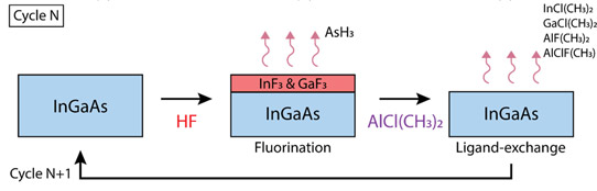
Figure 1: Proposed reaction mechanism of InGaAs thermal ALE.
The researchers applied the HF/DMAC ALE to InGaAs/InAlAs vertical nanowire (VNW) structures that were previously etched by a reactive-ion process involving boron trichloride, silane and argon. Before ALE the VNWs were 185nm high and 28nm diameter.
A 300-cycle 250°C ALE reduced the diameter of the InGaAs section to 24nm diameter, while the InAlAs was 18nm. The InGaAs section remained constant under 300 more cycles of ALE, but the InAlAs section reduced further to 10nm.
Increasing the ALE temperature to 300°C enabled thinning of 34nm-diameter VNWs to 24nm and 4nm for the InGaAs and InAlAs sections, respectively, after 250 cycles. The etch rates for InGaAs and InAlAs were 0.24Å/cycle and 0.62Å/cycle, respectively.
The team comments that the delicate structure with a 4nm-diameter stem is possible “because thermal ALE is a gas-phase process without a wet etchant”. The researchers add: “In contrast, conventional solution-based self-limiting etching techniques, such as the digital etch, can be destructive to fragile nanostructures.”
X-ray photoelectron spectroscopy (XPS) studies suggested that a gallium layer builds up on the etch front of the lower temperature ALE, which inhibits the process. The researchers point out that Gibbs free energy considerations make InAs fluorination more favorable than that for GaAs.
The ALE process was incorporated into a finFET fabrication flow. Dry etch was used to create 24nm-wide fins. An alcohol-based digital reduced the fin width by 1nm/cycle for eight cycles, before loading into the ALD tool for in situ ALE and ALD processing. A 300°C HF/DMAC ALE was run for 250 cycles. This cut through the InAlAs, leaving InGaAs fins suspended in space.
ALD was used to deposit 4.7nm Al2O3 and 20nm tungsten all-around gate stacks. Since the etch processes were crystal orientation-dependent, the fin sidewalls were chosen to be along the {011} direction.
The resulting finFETs were found to have fin widths as low as 3nm in the upper section and 4nm in the middle. The researchers comment that the ALE/ALD process results in much sharper metal-oxide-semiconductor interfaces, compared with a similar process without ALE. The team attributes this to the prevention of surface oxidation before the gate-stack deposition.
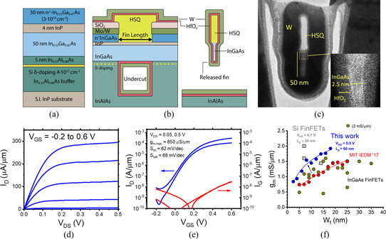
Figure 2: (a) Starting heterostructure for InGaAs n-channel FinFETs grown by MBE. (b) Cross-sectional schematics of FinFET along source-drain direction and across fin. (c) Cross-sectional transmission electron microscope image of finished FinFET with 2.5nm fin width. Inset: close-up of InGaAs channel. (d,e) Output and subthreshold characteristics of 2.5nm-width fin device. (f) Benchmark of maximum transconductance (gm) as function of fin width (Wf) for InGaAs FinFETs and state-of-the-art Si FinFETs. Blue data from latest work; red data from earlier heterostructure without in-situ thermal ALE and ALD.
Complete finFETs were fabricated in an ohmic contact-first, gate-last, self-aligned flow, using the in-situ ALE/ALD process (Figure 2). The hydrogen silsesquioxane (HSQ) hard mask used for patterned etching was not removed from the top of the fins. This means the gate was not strictly ‘all-around’ but rather formed an inverted trigate wrapping around the bottom of the fin.
The ohmic contacts were formed from molybdenum/tungsten (Mo/W). The gate stack used 3nm ALD hafnium dioxide (HfO2) as the dielectric – the equivalent oxide thickness was 0.8nm. The ALD W gate metal thickness was 30nm. The preceding ALE fin thinning was 162 cycles HF/DMAC at 300°C. Fin widths ranged from 180nm down to 2.5nm. The gate length was 60nm.
The 2.5nm fin width device demonstrated near-ideal linear (50mV drain) and saturation (0.5V) subthreshold swings of 62mV/decade and 68mV/decade, respectively. The ideal at 300K (room temperature) would be 60mV/decade – many InGaAs devices report around double or even more of that value. The drain-induced barrier lowering (DIBL) was found to be 40mV/V. The peak transconductance was 850μS/μm at 0.5V drain bias. The device was previously reported at the last IEEE International Electron Device Meeting in December 2018.
ALE FinFETs AlO InGaAs InAlAs InP substrate MBE
https://pubs.acs.org/doi/full/10.1021/acs.nanolett.9b01525
The author Mike Cooke is a freelance technology journalist who has worked in the semiconductor and advanced technology sectors since 1997.


