


- News
28 August 2019
Ferroelectric gate stack for normally-off gallium nitride power transistors
Taiwan’s National Chiao Tung University and Universiti Kebangsaan Malaysia (UKM) have used ferroelectric materials to create normally-off tri-gate gallium nitride (GaN) metal–insulator–semiconductor high-electron-mobility transistors (MIS-HEMTs) [Chia-Hsun Wu et al, IEEE Transactions on Electron Devices, published online 8 July 2019]. The researchers claim the lowest reported specific on-resistance for normally-off GaN transistors with breakdown voltages greater than 650V.
A hafnium oxynitride (HfON) ferroelectric layer in the gate stack was designed to trap charge that shifted the threshold voltage of the transistor to positive values, giving normally-off behavior – i.e. a low current flow at 0V gate potential. Normally-off behavior is desired to reduce power consumption, and in power applications to provide fail-safe operation with simpler circuits. A key trade-off in such devices is between low on-resistance and high breakdown voltage.
The tri-gate structure improved electrostatic control of current flow in the channel by wrapping the gate stack around fins etched out of the channel material.
The III-nitride materials were applied to silicon substrates using metal-organic chemical vapor deposition (MOCVD) to give a 20nm aluminium gallium nitride (Al0.3Ga0.7N) top barrier, 300nm GaN channel and 3μm carbon-doped GaN buffer. Carbon doping of GaN has been found to make it highly resistive.
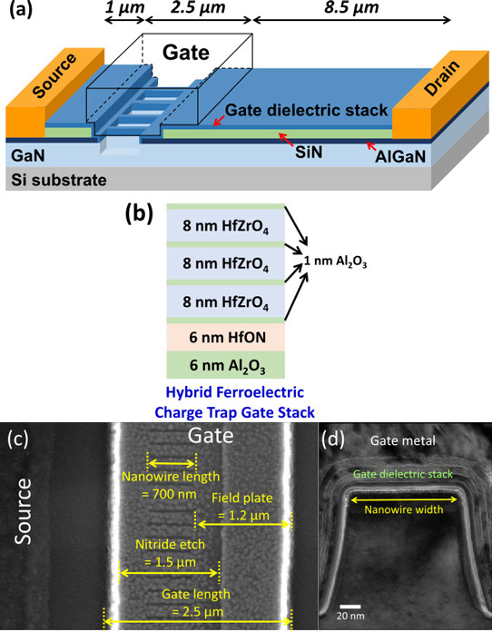
Figure 1: (a) Schematic cross section of GaN tri-gate device with hybrid ferroelectric charge trap gate stack. (b) Schematic cross section of gate dielectric stacks. (c) Top-view scanning electron microscope image of tri-gate device. (d) High-resolution transmission electron microscope image of single nanowire.
The fabricated devices (Figure 1) featured titanium/aluminium/nickel/gold ohmic source-drain contacts, nitrogen implant planar electrical isolation, inductively coupled plasma (ICP) etched 700nm-long fins/nanowires, 50nm plasma-enhanced CVD silicon nitride passivation, ICP etch of silicon nitride in the 1.5μm gate region, atomic layer deposition (ALD) of gate dielectric stack layers, 400°C annealing to crystallize the hafnium zirconium oxide (HfZrO4) in the gate stack, and electron-beam evaporation of the nickel/gold tri-gate.
The gate structure was designed to allow charge trapping in the HfON layer with tunneling through the bottom 6nm Al2O3 layer. A comparison planar structure without nanowire/fin etching was also fabricated. The overhang of the gate metal on the drain side was designed as a field plate to increase the breakdown voltage. The nanowire region of the transistor consisted of 119 fins of 140nm height, 100nm width, and 110nm separation.
The transistors were initialized with 12V applied to the gate, charging up the HfON trapping layer of the gate stack. The fin structure enables the charges to be closer to the GaN channel, separated by 6nm tunneling oxide on the sidewalls. This contrasts with the planar structure, and the top of the nanowires, where there is in addition the 20nm AlGaN barrier, giving a 26nm total.
The closer proximity of the sidewall charge trapping layer increases the threshold voltage of the transistor – +5.38V shift for the nanowire device, compared with a +3.80V shift for the planar gate with 5V drain bias. These shifts enabled a positive ‘normally-off’ threshold (Vth) for 1μA/mm drain current of +2.61V in the tri-gate device, compared with the negative ‘normally-on’ value of -5.28V for the planar transistor.
The team comments: “The tri-gate device demonstrated the highest Vth among the reported normally-off nanostructured GaN device results, this is due to a high density of negative charges stored in the hybrid ferroelectric charge trap gate stack.”
The tri-gate finFET also demonstrated better gate control with 73mV/decade subthreshold swing, compared with 83mV/decade for the planar structure. The hysteresis was slightly higher for the tri-gate transistor at 0.19V, compared with 0.1V for the planar device. The researchers blamed etch damage, creating interface traps on the nanowire sidewalls.
The gate leakage of the tri-gate device was 0.4nA/mm with the gate at 12V. The peak transconductance of the tri-gate transistor, 177mS/mm, was lower than that of the planar device, 208mS/mm, due to a lower drain current resulting from removal of more than 50% of the channel width in the fin region.
The maximum drain currents for the planar and tri-gate transistors were 1330mA/mm and 896mA/mm, respectively. The corresponding gate potentials were 10V and 14V. The on-resistance at these gate potentials at 0.5V drain bias were, respectively, 4.3Ω-mm and 5.0Ω-mm. Again, the removal of channel width by the fin etch explains the lower drain current and higher on-resistance of the tri-gate transistor.
The breakdown voltage for a leakage current of 1μA/mm was 788V with 0V gate in the tri-gate transistor. To give an off-state in the planar device, the gate was set at -8V; the resulting breakdown voltages was 738V. The researchers write: “Higher BV for the tri-gate device is due to the field-plate design associated with the tri-gate structure.”
The current collapse was investigated with the drain bias off-state stress up to 600V. The off-state time was 10ms. The dynamic on-resistance for 150μs pulses was 1.66x and 1.64x, compared with the DC value (0V drain stress), for the tri-gate/planar transistors, respectively. The on-state was measured with 12V on the gate and 1V drain bias.
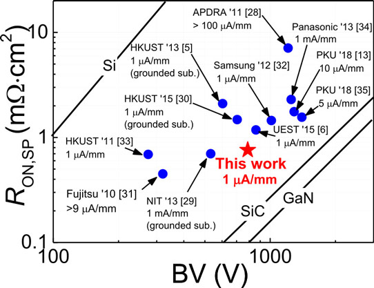
Figure 2: Benchmarking RON,SP versus BV data of tri-gate device with state-of-the-art normally-off GaN devices.
In benchmarking breakdown voltage (BV) against specific on-resistance (RON,SP) in other reports (Figure 2), the researchers comment: “To the best of our knowledge, the proposed tri-gate device shows the lowest RON,SP among reported normally-off GaN device results with BV >650V.” The RON,SP of the tri-gate transistor was as low as 0.76Ω-cm2.
One worry for the device would be high-temperature performance at~150°C. The team points out that the thermal risk of charge detrapping would lead to Vth instability worries. Similar concerns are raised by long-term gate-bias stress.
Ferroelectric GaN MIS-HEMTs HfON ALD MOCVD
https://doi.org/10.1109/TED.2019.2922301
The author Mike Cooke is a freelance technology journalist who has worked in the semiconductor and advanced technology sectors since 1997.


