


- News
19 December 2019
Deep UV aluminium gallium nitride laser diode at 271.8nm wavelength
Researchers from Japan and the USA claim the shortest wavelength so far reported for current-injection laser diodes (LDs) [Ziyi Zhang et al, Appl. Phys. Express, vol12, p124003, 2019]. The emission wavelength of 271.8nm places it in the deep ultraviolet (UV-C) 100-280nm range. Previous UV laser diode reports have been restricted to the 315-400nm UV-A range.
Asahi Kasei Corp and Nagoya University in Japan and Crystal IS in the USA collaborated on the device, which used low-dislocation-density aluminium nitride (AlN) substrates to grow layers of aluminium gallium nitride (AlGaN). Most reported short-wavelength laser diodes use silicon carbide, sapphire or freestanding gallium nitride as the growth substrate.
The team used an unintentionally doped distributed polarization-induced doping (DPD) cladding layer on the p-side, aiming for low internal loss, high hole conductivity and high hole injection. The usual magnesium doping of AlGaN has very poor performance in terms of generating mobile holes. Further, the use of ionized impurities creates scattering centers for light and charged carriers, which adversely impact performance.
UV-C emitting devices could have a wide range of applications: biochemical sensing, small-particle detection, disinfection, medical treatment and surface monitoring are mentioned in the paper. These very short wavelengths are able to disrupt biochemicals such as DNA with potential for disinfection and water purification of bacterial and viral pathogens.
The researchers grew the laser diode structure (Figure 1) on 2inch-diameter (0001) AlN substrates using metal-organic chemical vapor deposition (MOCVD). The dislocation density in the single-crystal substrate from Crystal IS was in the range 103-104/cm2. The 9nm light-emitting single quantum well was designed to emit 270nm wavelength UV-C light.
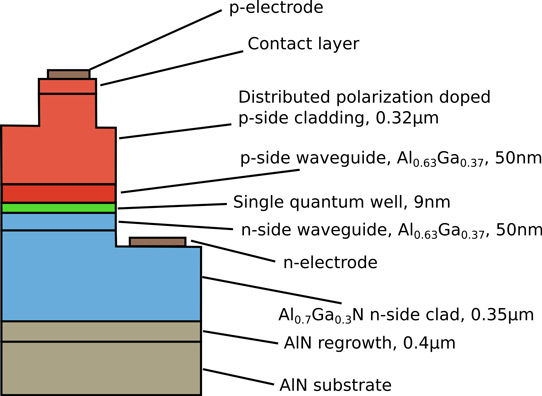
Figure 1: Schematic of fabricated UV-C laser diode structure.
The 0.32μm distributed polarization doped p-side cladding consisted of AlxGa1-xN graded from 100% to 70% Al content. The grading effects a charge polarization gradient that creates and conducts mobile holes. The p-contact region consisted of magnesium-doped AlGaN further graded down to pure GaN. The n-side of the device was doped with silicon using an impurity concentration of more than 1x10¹⁹/cm3 in both contact and cladding layers. The epitaxial layers were strained pseudomorphically with the underlying AlN substrate.
Laser diode devices were fabricated with 4μm-wide ridge waveguides. The ridge etch exposed the n-contact layer on which vanadium-based metal was deposited. Silicon dioxide passivation was applied before the n-contact metal. The p-contact and other wiring and probe pads consisted of nickel/gold metal.
The fabricated laser diodes were cleaved along the <11-20> direction into 400μm-long cavities. The resulting (1-100)-plane facets were coated with five dielectric layer pairs consisting of hafnium dioxide and silicon dioxide. The reflectivity of the coatings were more than 90%, according to the researchers. The high reflectivity was a key factor in reducing threshold current.
The laser diodes were tested under pulsed operation with 50ns width and 0.01% duty cycle. The light output power increased non-linearly at around 0.4A injection, 25kA/cm2 density relative to the p-electrode area. Above this threshold a sharp spectral peak emerged around 271.8nm wavelength. The threshold occurred with a forward voltage of 13.8V.
The optical polarization of the emission was transverse electric (TE): while the transverse magnetic (TM) component had a constant 11nm full-width at half maximum (FWHM) between 0.2A and 0.5A, the TE values were 6.6nm and 0.41nm, respectively (Figure 2).
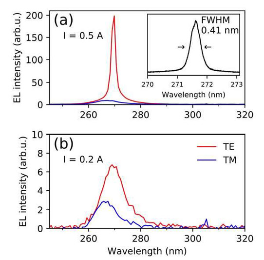
Figure 2: Edge emission spectra with TE and TM polarization at (a) 0.5A and (b) 0.2A forward current. Inset in (a) shows spectrum of TE mode at 0.5A with highest wavelength resolution.
The researchers attributed the “remarkably low” threshold voltage of 13.8V to the DPD structure giving a flat valence band profile on the p-side, allowing injection of the holes without a barrier. They also speculate that the high-Al-content material on the p-side of the waveguide layer created an electron-blocking barrier in the conduction band.
The team comments: “The pseudomorphic growth of the whole structure, including the DPD on the single-crystal AlN substrate, maximized the polarization-induced charge to achieve high hole conductivity, considering that relaxation of the graded structure can also hinder polarization doping.”
One problem was found in the MOCVD growth process: convex, hexagonal pyramid-shaped hillocks on the surface with a density of 6x10³/cm2. The hillocks seemed to contribute an additional emission peak around 278nm wavelength. In devices that included one of these hillocks, lasing was not achieved.
The researchers believe, based on transmission electron microscope analysis, that the hillocks originate from pre-existing threading dislocations in the AlN substrate. Threading dislocations offer non-radiative routes to carrier recombination and can adversely affect current flow patterns.
For lasing, the hillocks also affect the optical structure, scattering light out of the waveguide mode. “A high-quality AlN substrate with low dislocation density appears to be fundamental to the development of a UV-C LD,” the team concludes.
Deep UV laser diodes AlGaN AlN substrates MOCVD
https://doi.org/10.7567/1882-0786/ab50e0
The author Mike Cooke is a freelance technology journalist who has worked in the semiconductor and advanced technology sectors since 1997.


