


- News
26 December 2019
Toward photodetector arrays based on indium gallium nitride μLEDs
Fudan University in China and University of Toronto in Canada have been exploring the use of indium gallium nitride (InGaN) micro light-emitting diode (μLED) arrays in photodiode (PD) mode for multiple input, multiple output (MIMO) visible light communications (VLC) [Xiaoyan Liu et al, ACS Photonics, published online 31 October 2019]. The team suggests that the technology could lead to integration of display, fast data transmission and photodetectors, powered photovoltaically either through the signal itself or through solar illumination.
The researchers comment: “Such a multifunctional μLED information display is very useful for applications where high-speed wireless network and considerable electrical power are required, for instance information display chips for wearable virtual reality/augmented reality (VR/AR) devices, and outdoor large-screen display.”
VLC is seen as a wireless communication technology that could be deployed in environments where electromagnetic interference from radio frequencies could be problematic such as aircraft or hospitals.
The small size of μLEDs is expected to result in higher bandwidths due to smaller parasitic resistances and capacitances. Although single μLED photodetectors have been studied, the researchers report that parallel array structures of such devices have not been presented up to now.
The 2x2 MIMO system consisted of transmissions from 405nm violet laser diodes (LDs) transmitted over a free-space distance of 1m onto 450nm blue μLED structures used as photodetectors (Figure 1). The laser diodes were used due to reduced crosstalk between the two signal sources with reduced divergence angle of the beams. The laser light was collimated using lens systems.
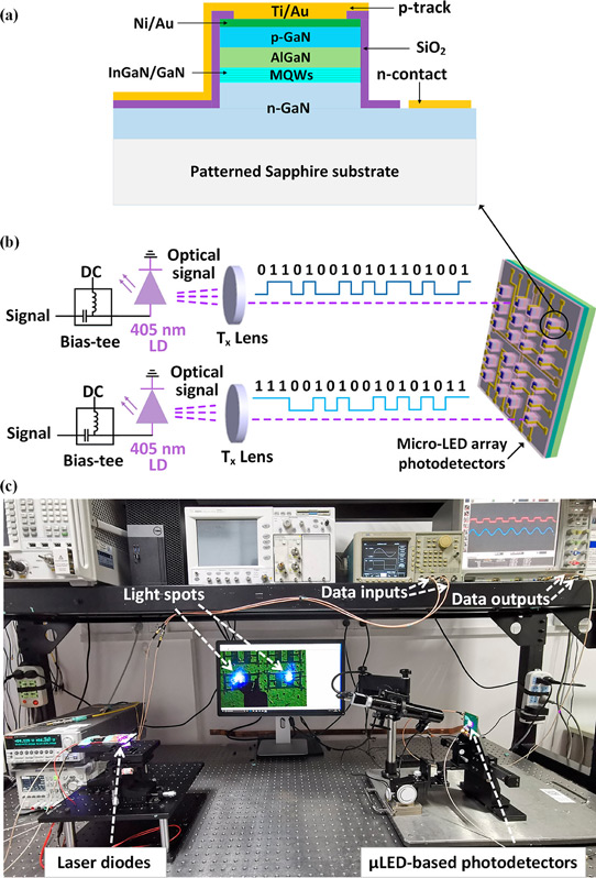
Figure 1: (a) Schematic diagram of μLED, (b) setup for MIMO VLC, and (c) photograph of experiment.
The researchers fabricated their devices using commercial metal-organic chemical vapor deposition (MOCVD) material grown on patterned sapphire substrates. The light-sensitive region was indium gallium nitride (InGaN) multiple quantum wells (MQWs) with GaN barriers. An aluminium gallium nitride (AlGaN) electron-blocking layer was included in the structure. The silicon dioxide (SiO2) insulation was applied using plasma-enhanced chemical vapor deposition (PECVD). Nickel/gold (Ni/Au) was used for current spreading. The n- and p-contact pads consisted of titanium/gold (Ti/Au).
The photodetector diameters varied between 40μm and 100μm. At zero bias, the photo/dark current ratio, or ‘photosensitivity’, was of order 109. This high value resulted from the very low dark current at zero bias of 10-14A. The laser diode power density reached as high as 11.0W/cm2.
With the devices biased at -5V, the photo/dark current ratio was 107 for the smaller devices, and 108 for the larger. The researchers say that these values match the best reported results and are “higher than previously reported values of the GaN photodetectors with photoconductive, p−i−n, or heterojunction structures”. The team expects the high values to benefit the signal/noise ratio and minimum detection limits of the devices.
When the illumination was at 11.0W/cm2, the short-circuit current was 27.4μA for the 40μm-diameter μLED. This increased to 188μA for 100μm diameters. The open-circuit voltages were all 2.6V. This photovoltaic effect could be used to power other parts of a circuit. The researchers report that they have used such harvested energy to power a 660nm laser diode. The team sees potential for such setups to be used in powering systems in hazardous and harsh environments.
The responsivity of the self-powered μLEDs with 11.0W/cm2 laser power density was 0.24A/W for 40μm diameters, and 0.21A/W for 100μm. A 60μm-diameter μLED achieved 0.29A/W response. The researchers estimate the quantum efficiency to be 74%, 88% and 62% for 40μm-, 60μm- and 100μm-diameter μLEDs, respectively.
Biasing the devices at -5V gives corresponding responses of 0.27, 0.31 and 0.24A/W – and quantum efficiencies of, in the same order, 82%, 96% and 73%. The researchers attribute the increased performance to the enhanced separation and collection of electrons and holes under reverse bias.
The team comments: “The values of responsivities are higher than that of a commercial Si-PIN photodetector at the wavelength of 405nm and are slightly better than the GaN-based photodetectors in previous reports without internal photocurrent gain.”
The specific detectivity that measures the effects of bandwidth and noise on the μLED-PD was around 1013Jones (cm-Hz1/2/W) at zero bias – 7.5x10¹²Jones for 40μm diameters and 1.5x10¹³Jones for 60μm. The values decreased somewhat for -5V bias due to increased dark current – 1.11x10¹¹Jones for 40μm and 2.3x10¹²Jones for 60μm diameters.
For high-speed communications, fast response to changes in illumination are needed. Smaller devices are likely to have faster rise and fall times. At zero bias, the rise and fall times in response to 11.7W/cm2 laser diode illumination were 22.0ns and 23.7ns, respectively, for the 40μm-diameter μLED. These times reduced with -5V reverse bias to 13.2ns and 13.7ns, respectively.
The researchers explain: “In comparison with 0V bias, the photoresponse time turns out to be shorter at a -5V bias, which is attributed to the increase of drift speed of carriers under reverse bias.
In fact, the 60μm-diameter μLED had improved rise/fall times: 17.2n/20.2ns at zero bias, and 12.2ns/12.7ns at -5V.
The -3db electrical-to-optical modulation bandwidths at -5V reverse bias were 56.8, 56.2 and 53.5MHz, respectively, for the 40μm, 60μm and 100μm devices. These values reduced at zero bias with corresponding values of 40.3, 41.2 and 38.6MHz.
In on-off keying (OOK) modulation transmissions, the researchers achieved 185 megabits per second (Mbps) with the 100μm device reverse biased at -5V (Figure 2). The bit error rate (BER) was 3.5x10⁻³, lower than the 3.8x10⁻³ upper limit for forward error correction (FEC) to be possible.
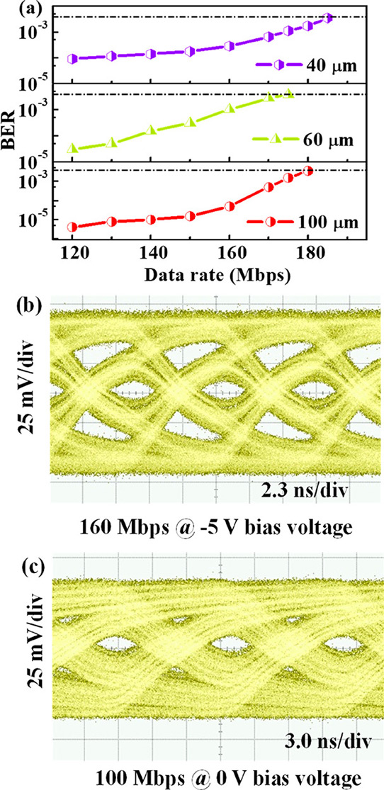
Figure 2: (a) BER versus data rate at -5V bias for μLED-based photodetectors with various diameters. Black solid line and black dash line represent -3dB bandwidth and FEC threshold, respectively. Eye diagrams captured at data rates of 160 (b) and 100Mbps (c) for 60μm μLED-based photodetector at -5V and 0V bias, respectively.
The 60μm device achieved 120Mbps with zero bias and 3.6x10⁻³ BER. Under -5V reverse bias, the same devices achieved 175Mbps and 3.7x10⁻³ BER. The researchers comment: “In the proposed 2x2 MIMO VLC, ideal real-time data rates of 350Mbps (under a −5V bias) and 240Mbps (under zero-bias) can be accomplished using 60μm μLED-based photodetectors as optical receivers.”
Applying scaling arguments, the team suggests that 18Gbps could be achieved with 10x10 arrays, and several terabits per second with 128x128 setups. However, “it is worth noting that there are significant challenges to achieve such extension to multi-Gbps transmission in practical applications because of the inevitable crosstalk and collimation difficulty for more and more arrays,” the team warns.
InGaN μLED Photodiode MIMO MOCVD PECVD
https://doi.org/10.1021/acsphotonics.9b00799
The author Mike Cooke is a freelance technology journalist who has worked in the semiconductor and advanced technology sectors since 1997.


