


- News
12 December 2019
Record power density aluminium gallium nitride barrier transistors
Researchers in France claim record power performance at 40GHz from aluminium gallium nitride (AlGaN)-barrier high-electron-mobility transistors (HEMTs) on freestanding gallium nitride substrates [Mohamed-Reda Irekti et al, Semicond. Sci. Technol., vol34, p12LT01, 2019]. The output power density reached 2W/mm with 20.5% power-added efficiency.
Although higher power densities have been achieved at lower frequency, the device from University of Lille, Laboratoire d’Analyse et d’Architecture des Systèmes, and Université Côte d’Azur, beat a previous high at 40GHz of 1W/mm.
The researchers used 2inch-diameter freestanding GaN substrates commercially produced by Saint-Gobain Lumilog via hydride vapor phase epitaxy (HVPE). The substrate had a resistivity of less than 30mΩ-cm.
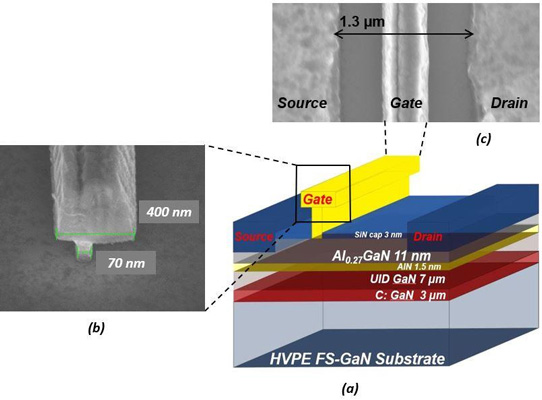
Figure 1: (a) Schematic of as-fabricated AlGaN/GaN HEMT on freestanding GaN substrate before passivation. Scanning electron micrographs: (b) after gate lift-off and (c) top view after gate fabrication
Metal-organic chemical vapor deposition (MOCVD) by the researchers added epitaxlial layers of 10μm resistive GaN buffer, 1.5nm AlN, 11nm Al0.26Ga0.74N barrier and 3nm in-situ silicon nitride cap (Figure 1). The resistive buffer was grown in two steps: 3μm carbon-doped GaN (C:GaN) and 7μm unintentionally doped GaN.
The exclusion layer aimed to reduce alloy scattering and enhance confinement of the electron carriers in the two-dimensional electron gas (2DEG) that formed the channel in the undoped GaN buffer near the interface. Hall-effect measurements gave 8.5x10¹²/cm2 electron density and 2200cm2/V-s. The corresponding sheet resistance was 356Ω/square.
The use of freestanding GaN substrates avoids the need for nucleation layers, which simultaneously create thermal barriers. Nucleation layers are needed when growing III-nitrides such as GaN on silicon carbide or silicon. These layers are highly dislocated to allow growth of lattice and thermal expansion mismatched materials.
The source-drain regions of the HEMTs were fabricated by argon-ion-beam etching more than half way through the AlGaN barrier layer and electron-beam evaporating and annealing titanium/aluminium/nickel/gold metal contact stacks. The etching brought the contact metals closer to the 2DEG channel, reducing access resistance.
The devices were electrically isolated using nitrogen-ion implantation. T-shaped nickel/gold gates were formed with a 70nm foot on AlGaN barrier. A 20-minute 400°C anneal was carried out in nitrogen to improve the Schottky contact, reducing trap states.
The devices were passivated with 340°C plasma-enhanced chemical vapor deposition (PECVD) of silicon nitride. Metal connections with the device contacts were made with titanium/gold evaporation and patterning.
The tested devices consisted of two 50μm-wide gate fingers in a 1.3μm source-drain gap. The source-gate distance was 500nm.
With the gate at 1V relative to the source, the maximum drain current was 950mA/mm, and the on-resistance was 3Ω-mm. The transconductance under 6V drain bias peaked at 300mS/mm, when the gate was at -2.5V. The threshold was -3.5V. The gate leakage was as low at 3x10⁻⁷A/mm, giving an on/off drain current ratio of more than 106.
Radio-frequency testing between 250MHz and 67GHz gave de-embedded/intrinsic gain cut-off frequency (fT) and maximum oscillation (fmax) values of 100GHz and 125GHz, respectively. The researchers believe that these parameters can be increased with optimization of the C:GaN layer, improving the trade-off between crystal quality and buffer isolation.
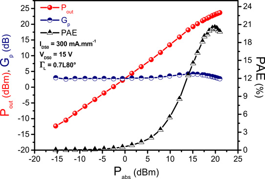
Figure 2: Output power, power gain and power-added efficiency versus absorbed power at 40GHz.
Power performance was assessed at 40GHz with active load-pull measurements under continuous-wave operation (Figure 2). The drain bias was 10V with the current at 300mA/mm, giving AB-class operation. The output power density was 1.2W/mm with 26.2% power-added efficiency. Increasing the drain bias to 15V, but keeping the current flow the same, increased the power density to a 2W/mm record, while decreasing the efficiency to 20.5%. The linear gain was 5dB with 10V drain, and 4.2dB at 15V.
The researchers comment: “Up to now, this result constitutes the state-of-the-art large signal at 40GHz for AlGaN/GaN HEMTs on freestanding GaN substrate.”
Freestanding GaN substrates AlGaN AlGaN HEMTs HVPE MOCVD
https://doi.org/10.1088/1361-6641/ab4e74
The author Mike Cooke is a freelance technology journalist who has worked in the semiconductor and advanced technology sectors since 1997.


