


- News
15 February 2019
Selective-area emitter for gallium nitride bipolar transistors
Researchers in China have improved the performance of gallium nitride (GaN) n-p-n heterojuction bipolar transistors (HBTs) on sapphire by growing the emitter layer selectively after the base and collector [Lian Zhang et al, IEEE Transactions On Electron Devices, published online 10 January 2019]. Selective-area growth (SAG) of the emitter layers avoids dry etch damage. Dry etch induces nitrogen vacancies and results in Schottky-type contacts for metal on p-GaN. The SAG enabled ohmic contact to the dry-etch-free p-type base layer.
The researchers at China’s Institute of Semiconductors and Microsystem and Terahertz Research Center suggest that, with optimized contacts and device scaling to smaller dimensions, such an HBT could be promising for radio-frequency power amplifiers for next-generation wireless communications. HBTs tend to have better linearity and higher current and power density, enabling high-power and high-temperature operation, compared with high-electron-mobility transistors and variants.
The epitaxial layers were grown on sapphire through metal-organic chemical vapor deposition (MOCVD): 2μm GaN buffer, 1μm n-GaN subcollector, 500nm GaN collector, and 70nm p-GaN base.
The selective-area growth was prepared with a patterned layer of plasma-enhanced chemical vapor deposition (PECVD) silicon dioxide. The emitter layer was grown in a window in the silicon dioxide – 50nm n-AlGaN grown at 980°C and 200Torr pressure. The aluminium fraction was measured at around 7%. In fact, the AlGaN thickness was 150nm at the window edge and 120nm in the middle. Atomic force microscopy (AFM) gave a root-mean-square roughness of 0.371nm in a 5μmx5μm area.
While the fabricated HBTs had a variety of emitter sizes, the metal contacts were placed at fixed distances from respective mesa edges – 2μm for the base and emitter metal to the base-emitter mesa, 2μm for the collector to the base-collector mesa, and 3μm for the base metal to the base-collector mesa.
An HBT with 20μmx20μm emitter area achieved 8kA/cm2 collector current density (JC) and 75kW/cm2 power density with collector-emitter voltages of 6.5V and 10V, respectively (Figure 1). “The high JC and power density benefit from the realization of base ohmic contact that increases base conductivity and consequently enhances base current injection,” the team comments.
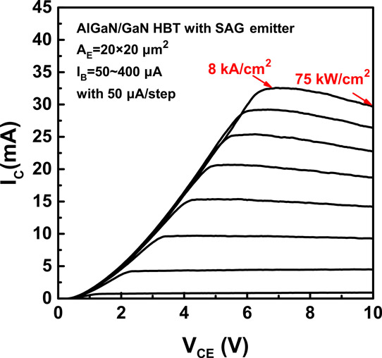
Figure 1: Common-emitter family curves.
The collector/base current gain was more than 80 when the base current exceeded 250μA. The maximum gain value of 90 for 0V base-collector bias was obtained at 7.7V base-emitter voltage (Figure 2). The base current was 0.23mA. The 90 gain is believed to be the highest among reported devices on sapphire. The offset and knee voltages of less than 0.5V and 6.5V, respectively, represent the lowest reported for GaN-based HBTs of similar area, according to the researchers.
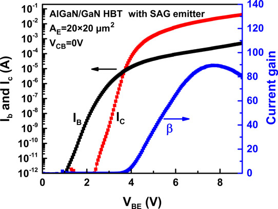
Figure 2: Gummel plot curves.
Devices with a larger emitter area had smaller gain values, likely due to defects at the base/emitter interface enabling tunneling.
The open-base breakdown voltage of the 20μmx20μm-emitter HBT was 98V with 1μA current compliance. The researchers believe that the voltage mainly dropped across the unintentionally doped GaN collector layer, giving an approximate breakdown field estimate of 2MV/cm, “comparable with reported direct-growth GaN-based HBTs”.
https://doi.org/10.1109/TED.2018.2890207
The author Mike Cooke is a freelance technology journalist who has worked in the semiconductor and advanced technology sectors since 1997.


