


- News
7 February 2019
Graphene-enabled aluminium gallium nitride nanopyramid arrays on silicon
Researchers based in Norway and Germany have grown aluminium gallium nitride (AlGaN) nanopyramid arrays using a graphene mask on silicon [A. Mazid Munshi et al, Appl. Phys. Lett., vol113, p263102, 2018].
The team from CrayoNano AS in Norway, Germany’s Max Planck Institute for the Science of Light and the Helmholtz Centre Berlin for Materials and Energy, and Norway’s SINTEF Industry and the Norwegian University of Science and Technology (NTNU) see potential applications for ultraviolet (UV) light-emitting diodes, photodetectors, and lasers. They hope that such material could overcome the problem of planar III-nitride structures of defects arising from lattice and thermal expansion mismatching. Graphene enables quasi van der Waals epitaxy, avoiding problems arising from dangling chemical bonds.
Sub-400nm-wavelength UV light is used in curing, sensing, food processing and microbial disinfection of water and air. For sterilization applications the wavelength restriction is even more stringent – less than ~250nm deep UV is needed in order to be able to disrupt DNA structures, for example. These very short wavelengths need AlGaN alloy material with high aluminium fractions. Until these problems are solved, systems will continue to rely on fragile, short-lifetime, toxic, bulky mercury lamps.
The single-layer graphene was grown by chemical vapor deposition (CVD) on copper foil and then transferred to 2-inch silicon (Si) substrates with native oxide layer. Electron-beam lithography was used to create a hole pattern in the graphene (Figure 1).
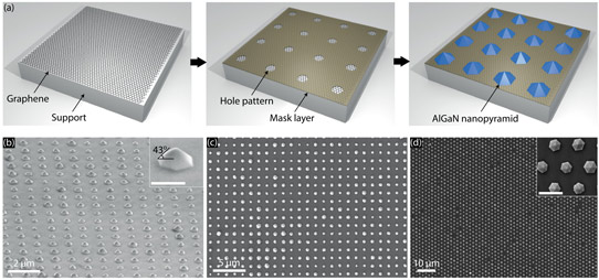
Figure 1: (a) Schematic of hole mask patterning and AlGaN nanopyramid growth on graphene. Tilted- (b) and top-view (c) scanning electron microscope (SEM) images of AlGaN nanopyramid arrays with 1μm-pitch square pattern showing good uniformity and very high nucleation yield. Inset (b): scale bar 400nm. (d) Top-view SEM image of AlGaN nanopyramid array with 2μm pitch trigonal pattern. Inset (d): scale bar 2μm.
The AlGaN nanopyramids were grown using metal-organic vapor phase epitaxy (MOVPE) with trimethylaluminum (TMAl), trimethylgallium (TMGa) and ammonia (NH3) precursors. Nitridation (optional) and nucleation, at 1200°C thermocouple reading, created islands from which nanopyramids were grown at 1150°C, with silane (SiH4) used for n-type doping. The researchers estimate that the growth surface temperature was about 100° less than the thermocouple reading.
The resulting nanopyramids had hexagonal bases. The side facets presented {10-12} planes from the crystal structure, giving a ~43° tilt angle to the substrate. “The formation of the {10-12} side-facets is caused by the slow growth rate along the <10-12> directions due to the low NH3 flow used for the nanopyramid growth,” the team explains. Some nanopyramids had poorly defined side facets – this was attributed to formation of multiple AlGaN crystal seeds on the nucleation layer that subsequently merged.
The photoresponse from electron-beam excitation – cathodoluminescence (CL) – gave a peak at 366nm (Figure 2). There was also very strong defect-related luminescence around 550nm. The 366nm peak seems to come from pure GaN band-edge emission, despite the presence of ~2.8% aluminium during growth. The researchers comment: “This indicates sub-optimal growth conditions with a reduced material quality, as evident also by the broad band-edge emission and strong defect luminescence, possibly caused by the use of low NH3 and high silane flows.”
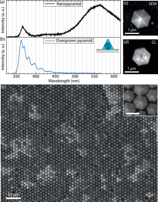
Figure 2: (a) and (b) Room-temperature CL spectra obtained from single pyramid from sample in Figure 1 (b) and (c) and from overgrown pyramid. Inset (b): schematic of whispering gallery mode formation. (c) and (d) SEM image and panchromatic CL intensity mapping of same pyramid. (e) Top-view SEM overgrown pyramid arrays of sample in Figure 1 (d). Inset: magnified view of sample; scale bar 2μm.
The low aluminium incorporation could be addressed in future by “modified growth techniques, e.g. pulsed-growth technique or using vertical flow MOVPE reactors”.
The researchers added MOVPE AlGaN/GaN/AlGAN heterostructures to the nanopyramids, with the AlGaN layers grown with 20% aluminium in the gas phase. The total overgrowth was around 300nm thick, according to transmission electron microscopy (TEM). The AlGaN layers were grown for 15 minutes each, while the GaN deposition lasted 1 minute.
CL from the overgrown material showed a peak around 363nm, along with a number of peaks on the longer-wavelength shoulder, likely “whispering-gallery-like modes”, according to the team. Defect-related emissions were not seen in this case.
The researchers comment: “This superior optical quality of the overgrown pyramids may be caused by the use of high NH3 flow leading to the formation of a very regular hexagonal shape with smooth side-facets.”
Cross-sectional TEM showed cavities at the bases of the nanopyramids, suggesting that the growth nucleates at the graphene edges of the holes.
AlGaN Graphene mask UV LEDs MOVPE CVD Silicon substrates
https://doi.org/10.1063/1.5052054
The author Mike Cooke is a freelance technology journalist who has worked in the semiconductor and advanced technology sectors since 1997.


