


- News
21 February 2019
First demonstration of fully vertical gallium nitride transistors on silicon
Switzerland’s École Polytechnique Fédérale de Lausanne (EPFL) has claimed the first demonstration of fully vertical gallium nitride (GaN) metal-oxide-semiconductor field-effect transistors (MOSFETs) on silicon (Si) [Riyaz Abdul Khadar et al, IEEE Electron Device Letters, online publication 22 January 2019].
Vertical devices are desired to take advantage of the large critical electric field, high electron mobility and saturation velocity, and high-temperature capability of GaN. Compared with lateral devices, vertical structures are more compact and the peak electric field tends to occur inside the bulk of the semiconductor rather than at surfaces.
Unfortunately, the vertical format has generally used prohibitively expensive bulk or free-standing GaN substrates to avoid leakage paths through threading dislocations. Use of silicon significantly reduces material costs, while the larger-diameter substrates should also lead to processing savings in mass production.
Some quasi-vertical devices have been produced on silicon with contacts arranged on the front-side of the wafer, similar to the way GaN LEDs on sapphire or silicon are powered. This leads to current crowding effects, increasing on-resistance.
GaN layers for the EPFL device (Figure 1) were grown by metal-organic chemical vapor deposition (MOCVD) on 6-inch (111) silicon: 1.07μm buffer, 1μm n-GaN, 4μm i-GaN intrinsic drift layer, 350nm p-GaN, 180nm n-GaN, and 20nm n+-GaN. Enkris Semiconductor collaborated with EPFL in the wafer growth processing.
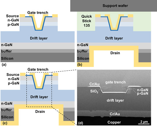
Figure 1: (a) Schematic of device structure after definition of source and gate pads. (b) Drain contact defined at back-side via support wafer attached using QuickStick 135 wax. (c) Schematic of completed device after removing support wafer. (d) Cross-sectional scanning electron microscope image of fabricated fully vertical GaN-on-Si MOSFET.
The resulting n-p-i-n structure was fabricated with 1.27μm gate trench dry etch and tetra-metal ammonium hydroxide wet treatment to remove etch damage. Rapid thermal annealing activated the p-GaN doping. Mesa etching to a depth of 1.35μm electrically isolated the devices. The gate oxide consisted of 100nm of atomic layer deposition (ALD) silicon dioxide. Dry etch of the silicon dioxide opened windows for chromium/gold source and gate contacts.
Back-side processing began with grinding the 1000μm-thick substrate down to 500μm. The wafer was then mounted on a silicon wafer with wax. Deep reactive ion etch (Bosch process) removed the silicon under the device, followed by dry etch of the resistive GaN buffer layer. An ohmic chromium/gold deposition made contact with the n-GaN drain. Electroplated copper in a 35μm-thick layer provided mechanically stable support for the GaN membrane. Acetone was used to release the device wafer from the mounting wax.
The researchers found the orientation and material of the etch mask for the gate-trench etch affected performance. Alignment along the m-plane, rather than a-plane, of the GaN crystal structure increased the current by up to 3x. “Such a significant enhancement is due to the much smoother m-plane sidewall after TMAH treatment compared to the a-plane,” the team comments. Using a nickel mask, rather than silicon dioxide, gave a further 1.6x boost to the drain current.
The nickel mask also increased effective channel mobility to 41cm2/V-s, compared with 21cm2/V-s for the oxide. The researchers comment that the 41cm2/V-s figure was “To the best of our knowledge,... the highest mobility reported on GaN trench gate MOSFETs grown on foreign substrates.”
One difference between the gate-trench etch results was the sidewall angle – 67° for the oxide mask, compared with 84° near-vertical for nickel. The team points out the the 67° angle for the oxide mask puts the surface close to the non-charge-neutral {10-11} GaN crystal plane.
The nickel-mask device achieved a drain current density of 1.6kA/cm2 and specific on-resistance (Ron,sp) of 5mΩ-cm2, both normalized to the active gate-trench area of the MOSFET (10μmx36μm), and accounting for a lateral 2μm current spreading from all sides of the trench. Compared with the EPFL’s previous work with quasi-vertical MOSFETs on a similar GaN epitaxial structure on Si substrate, the researchers report: “These devices exhibited 2.8x-better current density and 3x-lower Ron,sp.”
The p-GaN inversion channel is thought to be the major factor limiting performance, since other sources adding to the on-resistance are small.
The threshold voltage at 10V drain bias was 7.9V from linear extrapolation, and 6.4V according to the defined drain current density of 20A/cm2. The threshold is described as “relatively low”, “mainly due to donor-type N-vacancies present in the trench sidewall as a result of defects from the dry-etching process.” The MOSFET also suffered from a negative hysteresis of ~2V at 0.2kA/cm2 current density, “likely due to bulk oxide traps”. The team suggests that improving the oxide gate insulation and post-deposition annealing could reduce the hysteresis. The peak transconductance was 300S/cm2.
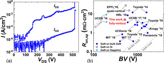
Figure 2: (a) Off-state blocking performance of metal mask vertical MOSFET measured at 0V gate potential. (b) Ron,sp versus BV benchmarking against other reported GaN vertical transistors on bulk GaN and Si substrates.
The off-state breakdown voltage (BV) was 520V (Figure 2). This is considered “excellent” by the researchers, who point out that the device did not use field reduction techniques such as field plates or edge termination structures. Breakdown was traced to the gate edge. The leakage current in the off state was less than 10-1A/cm2, normalized to the 110μmx197μm mesa area.
The researchers comment: “Compared to other GaN-on-Si transistors, our device presented a much lower Ron,sp of 5mΩ-cm2 and BV similar to previous reports on GaN-on-Si MOSFETs with a similar epitaxial structure and without field plates.”
https://doi.org/10.1109/LED.2019.2894177
The author Mike Cooke is a freelance technology journalist who has worked in the semiconductor and advanced technology sectors since 1997.


