


- News
14 February 2019
Boosting switching frequency in gallium nitride vertical fin transistors
Researchers based in USA and Singapore claim a record switching figure of merit for large-area 1.2kV gallium nitride (GaN) vertical power fin field-effect transistors (FETs) [Yuhao Zhang et al, IEEE Electron Device Letters, vol40, p75, 2019]. The team from Massachusetts Institute of Technology in the USA, Singapore-MIT Alliance for Research and Technology, and IQE RF LLC and Columbia University in the USA writes that this was “the first experimental study on capacitances, charges, and power-switching figure of merits (FOM) for a large-area vertical GaN power transistor.”
Vertical GaN structures should enable higher breakdown voltages in smaller dimensions with easier thermal management. The team reported on their design over a year ago at the International Electron Devices Meeting 2017 [www.semiconductor-today.com/news_items/2017/dec/mit_111217.shtml]. The device uses only n-type material, making for easier epitaxial growth and reducing charge storage problems. Normally-off performance is enabled by the fin structure in combination with the gate-metal work function producing full depletion of the channel at zero gate potential. Normally-off operation reduces power consumption and further allows for easy shut-off after failure.
The latest development of this device structure incorporated argon-implant edge termination under the gate pad edges “for the first time in vertical GaN FinFETs”.
The researchers used metal-organic chemical vapor deposition (MOCVD) on 2-inch heavily n-doped GaN substrates. The lightly doped n--GaN drift layer was ~9.5μm. The heavily doped n+-GaN cap was 300nm.
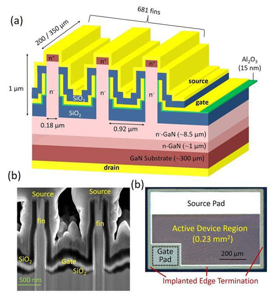
Figure 1: (a) 3D schematics of GaN vertical power FinFETs with multiple fin channels. (b) Cross-sectional scanning electron microscope (SEM) image of fin area, taken in focused ion beam system. (c) Optical microscope image.
The epitaxal material was fabricated into devices (Figure 1) with 489 350μm-long fins and 183 200μm-long fins (the gate pad region). The active device area was 0.23mm2. Adding pads and so on, increased the area to 0.45mm2.
The process sequence was fin etch and corner rounding, argon-implantation edge termination, spacer oxide deposition, and the formation of gate, source and drain contacts.
The resulting device had a threshold voltage of +1.3V at 2mA drain current. The researchers report that there was almost no hysteresis in the threshold with up and down sweeps. The drain current was able to reach 5A and the on-resistance was 0.9Ω, giving an active-area specific value of 2.1mΩ-cm2.
The reverse turn-on voltage was 0.8V, lower than usual for silicon carbide or gallium nitride devices (2-3V). The team attributes this to the absence of pn junctions in the epitaxial material. The low turn-on implies lower power losses and in some cases this could “eliminate the need for paralleling a freewheeling diode in many switching applications”. Destructive breakdown occurred above 1.2kV. Just before breakdown the leakage current was at the μA level.
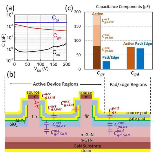
Figure 2: (a) Device junction capacitances Cds, Cgs and Cgd measured by using Agilent B1505A power device analyzer and custom-built RC circuit. (b) Schematics of different Cgs and Cgd components in active and pad/edge regions. (c) Calculated components break-out for measured Cgs and Cgd.
The researchers estimate that switching speeds for their device could reach ~3.5MHz on the basis of the on-resistance and charge storage performance. The greater the charge stored in parasitic capacitors (Figure 2), the more difficult it is to switch states. A figure of merit based on the product of the on-resistance and gate and gate-drain charge was calculated at 3.3nΩ-C. The researchers believe that this could be reduced to around 2nΩ-C if the contact pads were optimized. A low value should enable higher switching speeds.
The team also reports the FOM for other devices: 7.68nΩ-C for Cree’s CPM2-1200-0160B silicon carbide (SiC) MOSFET, 5.4nΩ-C for United SiC’s UJN1208Z JFET, 54.5nΩ-C for ON Semi’s NGTB15N120FLWG insulated-gate bipolar transistor (IGBT) and 48nΩ-C for Infineon’s IPD90R1K2C3 silicon CoolMOS device. These devices also have significant reverse-recovery charge storage (Qrr) problems due to the presence of p-type regions. Including this charge increases the FOMs to 24.48nΩ-C, 14.85nΩ-C, 429.5nΩ-C and 4488nΩ-C, respectively. By contrast, since there is no p-type material in the team’s FinFET, the reverse-recovery charge is effectively zero.
The researchers comment: “As shown, our device exhibited the best power switching FOMs among all 0.9-1.2kV power transistors. This is attributable to the combination of the superior physical properties of GaN and the merits of our vertical FinFET (small capacitances, low VG [gate potential] and no Qrr).”
https://doi.org/10.1109/LED.2018.2880306
The author Mike Cooke is a freelance technology journalist who has worked in the semiconductor and advanced technology sectors since 1997.


