


- News
28 February 2019
Vertical integration of gallium nitride nanowire transistor and light-emitter
Matthew Hartensveld and Jing Zhang of Rochester Institute of Technology in the USA claim the first vertical integration of nanowire gallium nitride (GaN) field-effect transistors (FETs) and indium gallium nitride (InGaN) light-emitting diodes (LEDs) [IEEE Electron Device Letters, published online 29 January 2019]. The integration enables voltage control of the light output from the device. Vertical integration allows for compact structures with easier fabrication than alternatives such as high-electron-mobility transistor (HEMT) combinations with LEDs.
Hartensveld and Zhang see potential for displays that need smaller pixels and higher efficiency than can be easily constructed using present-day thin-film transistor and liquid-crystal combinations. Conventional LEDs also have scaling and other difficulties.
Compact, efficient light emission is desired in virtual-reality and augmented-reality systems, and micro-LED and nano-LED structures would seem a perfect fit. The problem is in the driving and control of such devices, preferably in an integrated monolithic format.
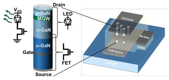
Figure 1: Schematic of vertical GaN nanowire LEDs with nanowire FETs. Inset: single wire and series connection.
Hartensveld and Zhang’s devices (Figure 1) consisted of 45 vertical nanowires each, on average. Heterostructured epitaxial material (Figure 2) was dry etched to create the wires – the so-called ‘top-down’ approach. The mask material for the chlorine reactive ion etch consisted of 3μm-diameter silica nanospheres spin-coated in deionized water onto the epitaxial wafer. Buffered oxide etch reduced the nanosphere diameters to 1.6μm. Dry etch damage was removed with a potassium hydroxide wet etch. The final nanowires were 5.5μm high and 1μm diameter.
Device contact fabrication built up layers of dielectric and metal. Transparent polydimethylsiloxane (PDMS) was spin coated, planarized and etched back to provide the dielectric spacing material for the various levels.
The titanium/aluminium (Ti/Al) source and drain contacts were applied in the same evaporation step to the bases and tops of the nanowires. Annealing (600°C 10m, 900°C 20s) was performed to form TiN, leaving behind nitrogen vacancies in the adjoining GaN. Such vacancies act as donors, releasing electrons for n-type conduction and giving an n-intrinsic-n (n-i-n) FET structure.
The all-around gate was formed from 40nm nickel evaporated about half-way up the undoped/intrinsic u-GaN region. The researchers see the use of this previously unused layer to give a ‘static induction transistor’ as a novel feature of their work.
The final fabrication steps include more spin-coated PDMS, etching and then evaporation of transparent indium tin oxide (ITO) conductor joining together the drain contacts of the individual nanowires, and etching to reveal buried device gate and source contacts.
The 1μm diameter of the nanowires was insufficient to fully deplete or pinch off the material under the Schottky gate at zero bias – therefore the transistor was not normally-off – a property desired for lower power consumption. It is hoped that narrower wires will lead to normally-off operation.
The switch-off of the ‘depletion-mode’ transistor came at -2.2V gate potential with the drain at 5V. The on/off current ratio was 2.9x10⁴, a 2.4x improvement over a 2014 GaN HEMT-LED report from Hong Kong University of Science and Technology (HKUST). There was some stepping in the current output of the Rochester device with increasing gate voltage, indicating the presence of unwanted trap states.
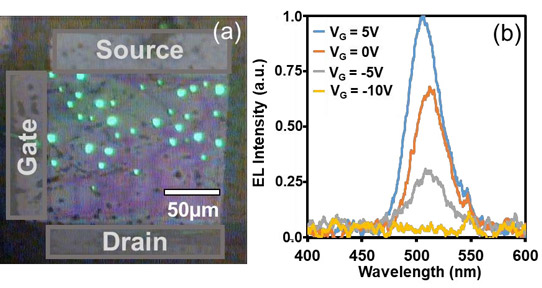
Figure 2: (a) Nanowire LEDs with FETs lighting up, and (b) electroluminescence spectra with gate modulation.
Due to the random distribution of the wires, the light intensity varied (Figure 2). It was found that clusters of wires shone more brightly than sparsely distributed ones. “Spin coating a close packed array or use of photolithography would allow high densities of ordered wires,” the researchers comment. The brightness was controlled by the gate potential – with 24V drain bias, the device was off with -10V on the gate, but as the potential increased the light emission increased.
GaN InGaN FETs LEDs Nanowire LEDs
https://doi.org/10.1109/LED.2019.2895846
The author Mike Cooke is a freelance technology journalist who has worked in the semiconductor and advanced technology sectors since 1997.


