


- News
30 January 2019
Reducing Schottky on-resistance in multi-channel III-nitride structures
Researchers based in Switzerland and China have reported on lateral Schottky barrier diodes (SBDs) using tri-gate multi-channel aluminium gallium nitirde (AlGaN) heterostructures on silicon [Jun Ma et al, IEEE Electron Device Letters, published online 17 December 2018].
École polytechnique fédérale de Lausanne (EPFL) and Enkris Semiconductor Inc see many possible applications for lateral devices with low on-resistance and high voltage blocking enabled by tri-gate structures. Such devices could include normally-on or normally-off transistors. Indeed, researchers from the same organizations recently reported on multi-channel tri-gate metal-oxide-semiconductor high-electron-mobility transistors [see Semiconductor Today, ‘Multi-channel tri-gate III-nitride high-electron-mobility transistors on silicon’].
The team comments: “This unique design significantly enhanced the device performance, leading to state-of-the-art lateral GaN-on-Si power SBDs, and unveiled a novel platform to drastically improve the efficiency, increase the current rating, and reduce the size of GaN-based power devices.”
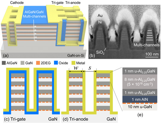
Figure 1: (a) Schematic of multi-channel tri-gate SBD. (b) Cross-sectional scanning electron microscope image of tri-gate region, tilted by 52°. Cross-sectional schematics of (c) tri-gate and (d) tri-anode regions. (e) Schematic of heterostructure composing each channel.
The multi-channel material consisted of 5 layers of 10nm/1nm/10nm AlGaN/AlN/GaN grown on silicon with a 4.3μm buffer layer (Figure 1). The AlGaN barrier layers were selectively doped with silicon. The sheet resistance of the structure was 230Ω/square with 5x10¹³/cm2 carrier density and 1820cm2/V-s mobility.
Fin structures were etched to enable access to the multi-channels. The nickel/gold (Ni/Au) Schottky anode comprised 200nm-high and 50nm-wide fins with 1.2μm oxide-insulated tri-gate and 4μm tri-anode regions. The tri-gate region served as a field plate to reduce peak fields and enhance breakdown performance. The gate structure also extended into the planar region, operating as a second field plate. The gate insulator was 25nm atomic layer deposition (ALD) silicon dioxide. The cathode-anode spacing was 15μm. The fins in the cathode region were 500nm wide with 500nm spacing.
A single-channel reference device was produced based on material with 1x10¹³/cm2 carrier density and 2000cm2/V-s mobility. The multi-channel device had ~50% reduced on-resistance (RON), compared with the single-channel performance. Also, the forward voltage for 0.1mA/mm current was reduced from 2.21V to 1.57V for the single- and multi-channel SBDs, respectively. The turn-on voltage of both devices was around 0.67V.
The reverse current of the multi-channel device (0.89nA/mm at -100V) was around six times smaller than for the single-channel structure. At 150°C, the reverse current at -100V was 86nA/mm for the multi-channel SBD.
With grounded substrate, the multi-channel SBD had a 1μA/mm breakdown voltage (VBR) of 900V. At -650V reverse bias, the leakage current (IR) was ~3nA/mm. “Such high voltage-blocking performance indicate the potential of these devices for 650V applications, providing a small IR at the rated voltage and a safety margin of ~50% from the rated voltage to the hard breakdown,” the researchers comment.
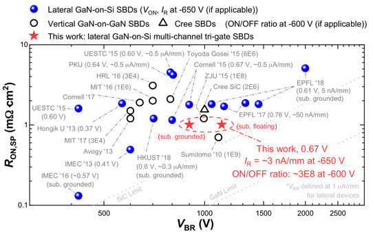
Figure 2: Specific on-resistance (RON,SP) versus VBR benchmark of multi-channel tri-gate SBDs against state-of-the-art lateral GaN SBDs. Some values were recalculated for fair comparison.
The VBR2/RON power figure of merit (FoM) was 1.25GW/cm2. The team says that this is comparable to state-of-the-art GaN-on-GaN vertical SBDs and GaN-on-silicon transistors (Figure 2).
The recovery times at 1MHz were 13.8ns and 8.2ns in the forward and reverse directions, respectively. These values were stable between 10kHz and 10MHz. However, a phase shift between voltage and current became apparent above 5MHz.
Lateral Schottky barrier diodes Tri-gate multi-channel AlGaN heterostructures AlGaN
Multi-channel tri-gate III-nitride high-electron-mobility transistors on silicon
The author Mike Cooke is a freelance technology journalist who has worked in the semiconductor and advanced technology sectors since 1997.


