


- News
17 January 2019
Gallium oxide prospects for high-voltage and high-power electronics
University of Florida and the Naval Research Laboratory (NRL) in the USA and Korea University have made a comprehensive review of the present and potential future status of gallium oxide (Ga2O3) electronics development [S. J. Pearton et al, J. Appl. Phys., vol124, p220901, 2018]. The paper covers 19 pages, with about 4 pages of references.
Although Ga2O3 semiconductor material has a number of potential benefits for high-power, and possibly radio-frequency, performance (Figure 1), the authors of the review see a number of hurdles to overcome. In the end, it is likely that Ga2O3 electronic devices will provide complementary capabilities to existing silicon (Si), silicon carbide (SiC) and gallium nitride (GaN) technologies. The review team sees Ga2O3 as possibly contributing in the low-frequency, high-voltage arena such as AC-to-DC conversion.
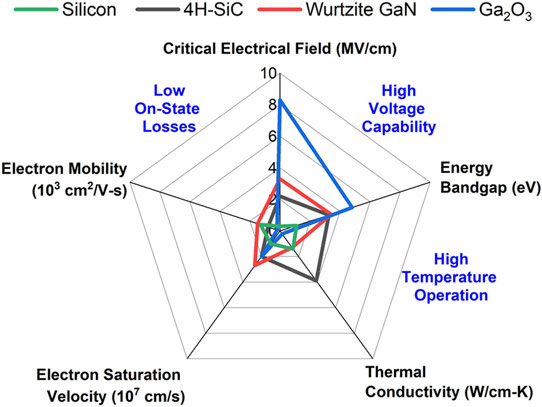
Figure 1: Pentagon diagram showing critical material properties important to power semiconductor devices. Larger pentagons preferred. Data from G. Liu et al, Appl. Phys. Rev., vol2, p021307, 2015; G. R. Chandra Mouli et al, IEEE Trans. Power Electron., vol50, p97-103,2018; B. J. Baliga, Semicond. Sci. Technol., vol28, p074011 2013.
Gallium oxide is a wide-bandgap semiconductor (~4.8eV compared with ~3.4eV for GaN, ~3.3eV for SiC, and 1.1eV for Si) that can be doped for n-type (electron) mobility in a controllable manner. Wide bandgaps are associated with high critical fields, allowing higher voltages and power densities to be handled before breakdown occurs. For Ga2O3, breakdown voltages up to 3kV have been reported.
A further attraction of Ga2O3 is the commercial availability of native substrates of the material at relatively low cost. This is based on the ability to use growth from molten gallium oxide to produce crystal material in the stable β polytype. It is crystal growth from silicon melt that enables high-quality substrates for mainstream electronics.
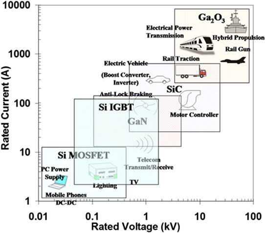
Figure 2: Applications for Si, SiC, GaN and Ga2O3 power electronics in terms of current and voltage requirements.
The team highlights “power conditioning systems, including pulsed power for avionics and electric ships, solid-state drivers for heavy electric motors, and advanced power management and control electronics” as potential applications (Figure 2).
Hurdles range from realizing usable, reliable components up to their insertion into sustainable market infrastructures. A big immediate drawback of Ga2O3, particularly in high-power-density applications, is a low thermal conductivity (10-30W/m-K versus SiC’s 330W/m-K, GaN’s 130W/m-K, and Si’s 130W/m-K). Thermal management strategies might include the transfer of device layers to another, more heat-conducting substrate, substrate thinning, heat sinks, top-side heat extraction, or active cooling with fans or liquid flow.
Another obstacle is the lack of a p-type doping mechanism. This is likely a fundamental problem, according to theoretical analyses. The reviewers report: “Self-trapping of holes in bulk Ga2O3, which decreases effective p-type conductivity owing to the resultant low mobility, is expected from the first-principles calculation of the Ga2O3 band structure. Theory indicates that all the acceptor dopants result in deep acceptor levels, which were not able to produce p-type conductivity.” Only at high temperature has there been any report of p-type conductivity, likely related to native Ga vacancy defects.
The reviewers suggest that combining n-Ga2O3 with other semiconductor materials with p-type conductivity might be possible. Copper iodide, copper oxide and nickel oxide may be in contention for this role.
The team suggests that the present market capacity is around 15-22 billion for discrete power devices. Making an analogy with the development of over some 35 years from conception to commercialization of SiC devices, they ask who will bear the costs for Ga2O3’s progress to the same state?
The reviewers comment: “A key requirement is continued interest from military electronics development agencies. The history of the power electronics device field has shown that new technologies appear roughly every 10-12 years, with a cycle of performance evolution and optimization. The older technologies, however, survive long into the marketplace, for various reasons. Ga2O3 may supplement SiC and GaN, but is not expected to replace them.”
The review adds: “Without an established revenue stream to support R&D over such a long time span, the clear driver has to be high-payoff military applications so that the necessary funding is there for long enough to truly develop this into a mature, manufacturable technology. It has never been the case with compound semiconductor power electronics that commercial applications have initially driven and sustained the development.”
Of course, these are views coming partly from the US Naval Research Laboratory. Further, the University of Florida team receives funding from the US Defense Threat Reduction Agency. However, it is undeniable that most of the early and continuing support of SiC and GaN power electronics development in the USA can be traced back to military research funding.
In Japan, where there has been some reluctance since World War II to be seen to engage directly in weapons markets, development of power technologies has been more focused on things like rail transport, electric motor vehicles, DC-AC conversion for renewable energy, power transmission (including high-voltage DC), control for electric motors in domestic appliances, and power supplies for consumer electronics.
The review sees the need for improvement in Ga2O3 development in seven areas: epitaxial growth, Ohmic contacts, thermally stable Schottky contacts, enhancement-mode (i.e. normally-off) transistor operation, the reduction of dynamic on-resistance, process integration, and thermal management through passive and active cooling.
The reviewers suggest that a breakthrough for Ga2O3 over the status quo is needed “in order to give it at least one application which will motivate R&D in the years to come.”
https://doi.org/10.1063/1.5062841
The author Mike Cooke is a freelance technology journalist who has worked in the semiconductor and advanced technology sectors since 1997.


