


- News
22 January 2019
Rockley completes silicon photonics platform in large-scale foundry environment
Rockley Photonics of Pasadena, CA, USA (formed in 2013 to develop a silicon photonics platform for optical I/O in next-generation sensor systems and communications networks) has announced the completion of its fully integrated silicon photonics platform running in a large-scale foundry environment.
Rockley says that it has overcome significant technological challenges that have, until now, held back the broad adoption and implementation of integrated photonics in high-volume applications. Chip-set shipments to customers have begun, and products implementing them will ramp up the production curve.
Delivering low-cost, high-value wafer-scale processing, the integrated photonic platform is key to product opportunities in applications where Rockley has go-to-market partnerships including optical sensing, 3D laser imaging and artificial intelligence (AI) computing connectivity. It is said to solve the key issues experienced by wafer-scale silicon photonics to date, including the elimination of active precision fiber alignment, full functionality in a single chip and optimized integration with microelectronics and systems.
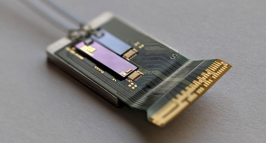
Picture: Rockley’s transmit-receive optical sub-assembly (TROSA) for data communication AOCs and transceivers.
“In one partnership example, active optical cables (AOCs) and transceivers will be manufactured by our joint venture with Hengtong Optic-Electric Suzhou, a world-leading optical fiber and cable provider,” says chairman & CEO Andrew Rickman. “The platform-derived photonics and electronics chip-set we are providing are key to facilitating the massive scaling required in data-center expansion, AI computing connectivity and 5G backhaul, where high bandwidth and dense optical input/output are paramount and also where cost and power utilization are critical,” he adds.
High-density in-package optical connectivity for powerful application-specific integrated circuits (optoASICs) - integrating optical connectivity directly with digital silicon CMOS within the same package - is one of the applications for which Rockley’s versatile technology platform has been developed. At last March’s Optical Fiber Communications conference (OFC 2018), Rockley demonstrated this technology in what was claimed to be the first single-ASIC Level 3 data-center routing switch with integrated 100G network ports using single-mode optical fiber.
“The platform’s ability to fully integrate transceiver functionality sets it apart from other transceiver solutions that use older chip-on-board, labor-intensive assembly practices,” says Rickman. “Its versatility provides the pathway for the vertical integration of a low-cost, differentiated product set that will help drive new competitiveness in large established markets like the AOC/transceiver market as data links reach 400G and beyond.”
Rockley’s wafer-scale platform includes the following functional blocks:
- Lasers - Multiple laser types (including back reflection tolerant and ultra-narrow linewidth) can be multi-channel and tunable, with good power efficiency over a wide optical bandwidth.
- Detectors – High-performance detectors for direct and coherent applications (including sensing and 400G communications).
- Modulators - Ultra-compact amplitude and phase modulators (which are power efficient, high speed and capable of handling a broad range of wavelengths for sensing and 400G applications).
- Free-space optics - The platform allows for efficient light coupling from free space into and out of the photonics circuits, with either edge or perpendicular coupling (enabling a broad range of 3D consumer-sensing applications).
- Fiber-optic coupling - Where needed, the photonic IC contains on-chip embedded ultra-efficient interfaces to optical fibers via single-step passive fiber-array attachment (allowing the fibers to be attached directly to the photonic IC without need for costly single-fiber active alignment process steps).
- Complex optical signal processing (waveguide circuits) - Optical circuits that are low loss, polarization maintaining and athermal for optical signal processing, CWDM/DWDM (coarse and dense wavelength-division multiplexing), coherent and high-resolution beam shaping, scanning and steering.
- Photonic integrated circuits - The platform enables integration of light sources, semiconductor optical amplifiers (SOAs), active devices, passive devices and optical coupling elements into a single silicon device (covering a wide optical band suitable for connectivity and sensing applications).
- Wafer-scale processing - The platform enables high-throughput wafer-scale processing of monolithic and multi-die structures (including chip-on-wafer integration).
- Interface electronics (ICs) – Rockley says that its electronics team has expertise in designing and delivering efficient and high-performance analog and mixed-signal ASIC blocks together with application-specific digital interfaces. The platform includes 2D and 3D packaging of photonics ICs with ASICs.


