


- News
9 January 2019
Mid-infrared aluminium gallium nitride quantum cascade detector on silicon
Technion-Israel Institute of Technology and Singapore's Nanyang Technological University (NTU) claim the first demonstration of an aluminium gallium nitride (AlGaN) quantum cascade detector (QCD) grown on 4-inch-diameter silicon substrates [Ben Dror et al, IEEE Electron Device Letters, published online 7 December 2018]. The detection wavelength was in the mid-infrared range (3-8μm). The long wavelength was enabled by inter-sub-band transitions (ISBTs) in the quantum cascade structure.
The team comments: “The successful implementation of [a] GaN ISBT optoelectronic device on silicon is promising [for] integrated-optoelectronics technology, showing great potential for ultra-fast operation at a very wide spectral range.”
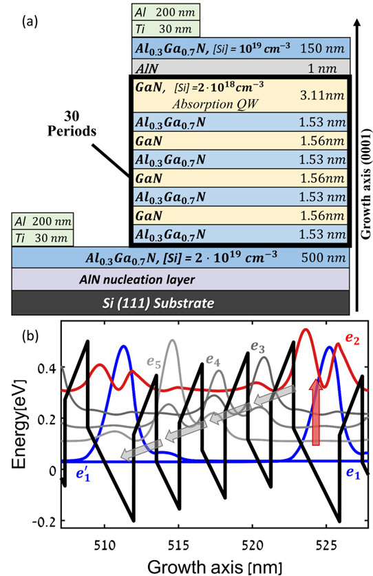
Figure 1: (a) Schematic of QCD structure. (b) Calculated conduction-band profile of 1.5 period of QCD's active area and shifted squared envelope functions of electronic bound states. Red vertical arrow indicates optical transition; gray arrows indicate transport direction of electrons in extractor region.
The QCD (Figure 1) was based on a 30-period cascade structure with an inter-sub-band transition energy of 267meV, corresponding to 4.49μm wavelength. The electron flow between stages was facilitated by longitudinal optical (LO) phonon-assisted tunneling. Infrared excitation of the structure produced a photovoltage.
The AlN/Si (111) 4-inch-diameter templates for the QCD structure were prepared by metal-organic chemical vapor deposition (MOCVD). The device layers were added by plasma-assisted molecular beam epitaxy (PAMBE) at 720°C.
Devices were fabricated on 7mmx7mm pieces diced from the epitaxial wafer. Mesas measuring 700μmx700μm were etched by inductively coupled plasma. The metal contacts consisted of titanium/aluminium (Ti/Al). The center of the top of the mesa was kept clear of contact metal as a window for front illumination into the absorbing layer.
The determination of the peak detection wavelength was hampered by the nearby presence of carbon dioxide absorption at 4.3μm (Figure 2). The researchers extracted a peak value of 4.14μm at 18K, red-shifting to 4.5μm at 150K. The 18K detection linewidth was 1.26μm full-width at half maximum (FWHM). The peak response also declines with increasing temperature, apparently disappearing into noise above 150K.
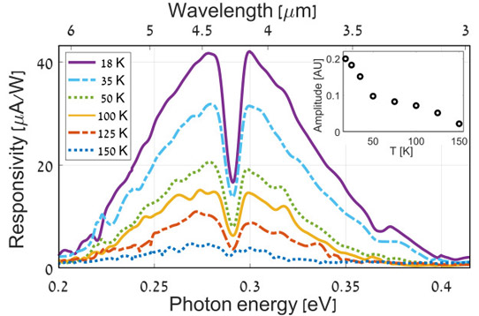
Figure 2: Spectral response of device. Dip is due to CO2 absorption. Inset: temperature dependence of signal is shown – peak signal at 18K.
Absolute responsivity was measured using a 1000K silicon carbide globular blackbody source. At 18K, a measured photocurrent of 162pA corresponded to a 44μA/W response. The detectivity, which incorporates the responsivity, the area of the blackbody aperture, and the current noise spectral density (15.4fA/Hz1/2), was 2x10⁸Jones at 19K.
The researchers suggest a number of potential improvements: optimizing the trade-off between absorption, extraction efficiency and resistance; reducing unwanted diagonal transitions from the ground state to the extractor quantum wells, increasing resistance and decreasing dark current; enhancing electron transport by tailoring the energy levels in the extraction stage to the LO-phonon ladder; and, increasing the doping to boost electron density in the quantum well for greater absorption.
Mid-infrared quantum cascade detector AlGaN
https://doi.org/10.1109/LED.2018.2885611
The author Mike Cooke is a freelance technology journalist who has worked in the semiconductor and advanced technology sectors since 1997.


