


- News
18 July 2019
High-electron-mobility III-nitride on 3C silicon carbide template on silicon
Germany’s Fraunhofer Institute for Applied Solid State Physics (IAF) reports on progress in growing III-nitride heterostructures on 3C polytype silicon carbide (SiC) on silicon substrates [Stefano Leone et al, J. Appl. Phys., vol125, p235701, 2019]. The team wanted to show that such heterostructures could achieve comparable electrical characteristics to epitaxial layers on 4H SiC substrates.
III-nitride heterostructures are used in high-electron-mobility transistors (HEMTs) aimed at high power density and/or radio frequency (RF) performance. These heterostructures consisting of aluminium (AlN) and gallium (GaN) nitride alloys are typically grown on 4H polytype SiC. Although 4H-SiC has many attractive features for high-power RF applications such as small lattice mismatch and small thermal expansion mismatch as well as and high thermal conductivity, substrates are prohibitively expensive.
The 3C-SiC on Si option promises to reduce material costs and provide economies of scale from much larger-diameter substrates (300mm versus 100mm). GaN has better lattice and thermal expansion match ups with 3C-SiC compared with silicon. In terms of thermal expansion, GaN’s coefficient is 5.6x10⁻⁶/K, which compares with 2.6x10⁻⁶/K for Si and 4.5x10⁻⁶/K for 3C-SiC. The lattice parameters for GaN and the (111) planes of Si and 3C-SiC are 0.319nm, 0.384nm and 0.329nm, respectively.
The researchers comment: “We believe that, by developing the material quality and characteristics of the 3C-SiC templates, we could transfer our optimized epitaxial process on such templates and make more cost-effective HEMT heterostructures available for the RF market.”
The III-nitride metal-organic chemical vapor deposition (MOCVD) was carried out on 100mm-diameter 3C-SiC on Si substrates supplied by three companies. The silicon was (111) oriented. The 3C-SiC layers were targeted to be around 2μm thick, variously doped n- and p-type. The n-type doping was unintentional, while boron provided the p-doping. The researchers also wanted semi-insulating and thicker 3-C SIC substrates, but such was unavailable from the suppliers at the time. Also, only one supplier was able to supply wafers with crack-free 2μm SiC.
Semi-insulating 3C-SiC is much desired for RF applications targeting the 10-100GHz range, particularly for AlGaN/GaN HEMTs in millimeter-wave monolithic module integrated circuits (MMICs). The team reported that it was working with the vendors, targeting crack-free 20μm thick semi-insulating 3C-SiC layers on highly resistive silicon substrates.
“Since the paper was accepted,” Stefano Leone, the lead author, reports, "we have now managed to get semi-insulating 3C-SiC layers with highly resistive substrates, and we have manufactured some transmission line model (TLM) structures with a great RF performance."
The MOCVD tool used in the epitaxial research was capable of holding multiple wafers and performing in-situ process monitoring. The group-III metals Ga and Al were supplied using trimethyl precursors. The nitrogen came in ammonia (NH3) molecular form. The carrier gas was hydrogen. Insulating GaN was created using iron doping with ferrocene (bis-cyclopentadienyl-iron (C5H5)2Fe) precursor.
The deposition was carried out at low pressures of 50-300mbar. Temperatures were in the range 1000-1200°C. The layer sequence was aimed at high-electron-mobility channel formation: nucleation, strain management, iron-doped insulating GaN, unintentionally doped GaN buffer, AlGaN barrier, and GaN cap. The researchers achieved smooth 5μm-thick epitaxial layers on 2μm-thick 3C-SiC without cracks. The wafer bow could be reduced to less than 50μm (Figure 1).
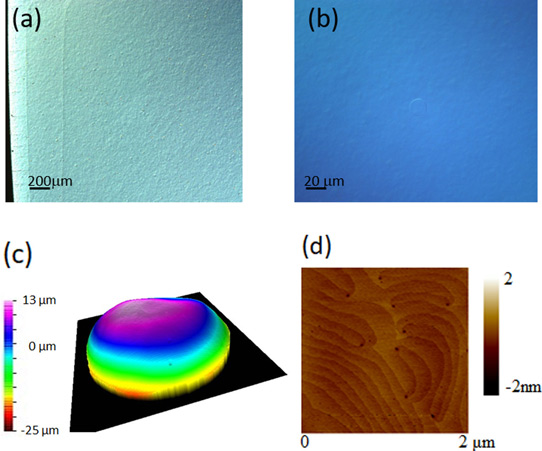
Figure 1: Morphology of 5μm-thick AlGaN/GaN epitaxial structure deposited on 3C-SiC/Si template, and images obtained by optical microscopy at: (a) 50x (wafer edge visible on left), (b) 500x magnifications, (c) three-dimensional plot of wafer bow, equal to +30μm, and (d) atomic force microscopy on 2μmx2μm area with 0.13nm root-mean-square roughness.
Low-temperature AlN interlayers were inserted into the GaN buffer to reduce wafer curvature and avoid cracking of the epitaxial layers. The AlN was used to counteract strain effects arising from thermal expansion and lattice mismatching with the underlying substrate. The researchers hope in future to implement a thick AlGaN transition layer approach on 3C-SiC/Si that is usually used in depositing on silicon for gradual transition from the compressive stress of the substrate to the GaN buffer layer. This would remove the need for the AlN interlayers, improving the GaN crystal quality and material properties.
The researchers report: “One of the main findings was that slow temperature ramps and a moderate desorption temperature were necessary to prevent cracking of the 3C-SiC layer itself. Nitridation of the surface, rather than an Al-preflow, led to better crystal quality. A thin nucleation layer (<60nm) of pure AlN or even Al0.7Ga0.3N proved itself to be good enough to achieve a good crystal quality of the GaN layers, while keeping a good strain management of the epitaxial structure.”
Table 1: Characteristics of similar HEMT structures deposited on different substrates.
| 4H-SiC | Si (111) | 3C-SiC/Si(111) | ||
| Structural characteristics | FWHM GaN 00.2 (arcsec) | 130 | 600 | 350 |
| FWHM GaN 10.2 (arcsec) | 180 | 900 | 650 | |
| Bow (μm) | 10 | 30 | 30 | |
| Electrical characteristics | Nmin (/cm3) | 1.3x10¹⁰ | 7x10¹² | 1x10¹³ |
| Ns (/cm2) | 6x10¹² | 4x10¹² | 9x10¹² | |
| Rs Ω/square) | 390 | 681 | 310 | |
| μ (cm2/V-s) | 1530 | 1360 | 1400 |
High-electron-mobility structures with more than 10nm barrier and cap with Al content around 30% was subjected to capacitance-voltage and Hall measurement characterization (Table 1) to extract sheet carrier density (Ns), minimum carrier concentration (Nmin), sheet resistance (Rs) and mobility (μ). These results were compared with structures on 4H SiC and (111) Si.
The 4H-SiC had an Nmin value three orders of magnitude lower than the 3C-SiC/Si sample. The researchers suggest that this is due to a higher density of dislocations and stacking faults, as indicated by x-ray analysis showing narrower full-width at half maximum (FWHM) values for rocking curves for diffraction off the 00.2 and 10.2 planes.
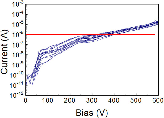
Figure 2: Vertical buffer isolation mapping’s measurement across GaN on 3C-SiC-HEMT epiwafer, using 75μm-diameter circular ohmic contact. For 1μA vertical current, isolation voltage is in the range 310V and 410V.
The team comments: “The outcome of this study is that the lateral isolation of the GaN buffer is good and similar to what is achieved on 4H-SiC, and the vertical isolation of the buffer is suitable for RF applications [Figure 2]. A big role in achieving this target is probably played also from the material quality of the GaN layers, which can be further improved by tuning the epitaxial growth conditions and also by having 3C-SiC templates with higher crystal quality, and especially a lower density of dislocations and stacking faults, which are known to be present in high density on 3C-SiC layers.”
The researchers also suggest that vertical high-power devices with 650-1200V ratings could be possible with low-carrier-concentration GaN buffers with improved vertical isolation capabilities on conducting 3C-SiC/Si substrates.
SiC substrates HEMTs AlN GaN MOCVD
https://doi.org/10.1063/1.5092653
The author Mike Cooke is a freelance technology journalist who has worked in the semiconductor and advanced technology sectors since 1997.


