


- News
31 July 2019
Indium arsenide and gallium antimonide fins on 300mm silicon
The Imec microelectronics research center in Belgium has been assessing indium arsenide (InAs) and gallium antimonide (GaSb) growth in shallow trench isolation structures on 300mm-diameter silicon substrates [Y. Mols et al, J. Appl. Phys., vol125, p245107, 2019]. The team sees the resulting fins as potentially forming the basis for vertical nanowire (VNW) tunnel field-effect transistors (TFETs).
The researchers are seeking ways to implement complementary metal-oxide-semiconductor (CMOS) ultra-large-scale integration (ULSI) using high-mobility III-V materials such as InAs and GaSb on a large-diameter silicon platform. The aim is to deliver high drive currents at low supply voltage, reducing power consumption.
Such applications require high-quality crystalline material. A big challenge to this is the large lattice mismatch of at least 8% between the III-V materials and silicon. The mismatch results in the generation of many defects in the growing crystal structures to relieve built-up strain.
One technique that has been used to block these defects from reaching the device levels has been aspect ratio trapping, where the crystal growth is initiated in trenches. The defects propagate to and terminate at the trench wall.
Fin structures are used in gate-all-around transistors and, it is hoped, in future vertical nanowire TFETs. The vertical transistor structure should result in even more compact circuitry.
IMEC performed metal-organic vapor phase epitaxy (MOVPE) on 300mm silicon wafers with silicon dioxide shallow trench isolation structures with V-grooves at the base presenting {111} facets of the underlying silicon crystal structure. The silicon wafer was (001) oriented and p-type doped.
The device areas were partitioned into 600μmx600μm blocks with different trench formations. The main work for the paper focused on 100nm-wide trenches. The trench length was 10μm.
The III-V seed was formed in the groove by first introducing tertiarybutylarsine (TBAs) in the MOVPE reactor, followed by the group-III metal (Ga, In) in trimethyl form (TMGa, TMIn). InAs fins were seeded at 380°C, followed by a ramp to 530°C. At the same time, the V/III ratio was reduced from 60 to 45. Once the trench was almost full, the temperature was reduced to 480°C in a TBAs environment. The final InAs fin had a flat (001) top surface.
For GaSb fins, direct growth on silicon either failed or resulted in poor-quality material. Instead, GaSb fins were grown on top of 150nm gallium arsenide (GaAs) deposited in two steps, with the low-temperature step having a V/III ratio of 50. The high-temperature GaAs buffer was grown at 580°C with a V/III ratio of 15. The top surface was (001). The antimonide growth was at 500°C or 530°C. The temperature ramp to the lower value was carried out under TBAs. The V/III was around 1 for the GaSb deposition.
The researchers comment that the GaSb long-range quality was poor. They attribute this to the 8% lattice mismatch between GaAs and GaSb. Further, the trench was effectively shallower for GaSb growth, reducing aspect ratio trapping effects. The higher growth temperature of 530°C reduced the pit/defect density per length of fin from 1.8/μm to 0.3/μm.
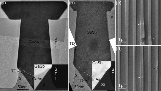
Figure 1: (Stitched) Cross-section TEM images of GaSb on (a) GaAs and (b) InAs seed. Dashed line at left bottom half of the V-groove is a guide to the eye, indicating the GaSb/seed interface. High-angle annular dark-field (HAADF) scanning transmission electron microscopy (STEM) overlay at bottom right half of the V-groove in both images clearly shows contrast difference for the GaAs/GaSb interface; using the dashed line one can also vaguely distinguish the InAs/GaSb interface. Top-view SEM of GaSb fins on (c) GaAs and (d) InAs seed. Black arrows indicate pits and white arrows the potential sites where along-trench stacking faults or nano-twins reach the surface.
To increase the aspect ratio for GaSb growth, the team performed antimonide MOVPE on low-temperature GaAs and InAs seed layers (Figure 1). During the ramp up to 530°C for the GaSb growth, the V-shape of the seed layer relaxed to a more rounded shape. The new setup resulted in a reduction in pit density to 0.03/μm along the fins with both types of seed.
To study conductivity properties, the researchers added silane (SiH4) as silicon precursor to the growth, giving n-InAs and p-GaSb doping. Scanning electron microscopy (SEM) bar regions were produced with 5mm-long trenches of various widths.
These were used for micro-4-point-probe (μ4PP) measurements on a microHALL-A300 tool from Capres (www.capres.com/Default.aspx?ID=59). The n-InAs fins were grown at 500°C on undoped low-temperature InAs seeds; the p-GaSb at 530°C on undoped low-temperature InAs or GaAs seeds.
An injection current of 1μA was used. The resistance results were normalized using the dimensions of the fins to give resistivity values (Figure 2). Increased doping reduced resistivity. In turn, the resistivity was not changed by growing the fins in wider trenches.
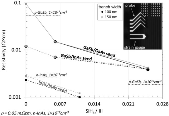
Figure 2: Measured resistivity for GaSb and InAs fins as a function of SiH4/III (III = TMGa or TMIn) and trench width (lines are a guide for the eye). Dashed-dotted lines represent some simulated resistivities needed for vertical nanowire TFET operation. Inset: μ4PP (8μm interprobe distance) and strain gauge contacting fin. Fins represented by darker lines with location indicated by dashed lines; lighter lines oxide.
Simulations suggest that the resistivity for source/drain regions of vertical nanowire TFETs with InAs fins should be of the order 0.00005Ω-cm. The demonstrated InAs fins achieved 0.001Ω-cm, a factor of 20 too high. The simulations suggest that InAs channels need the resistivity to be less than 0.0027Ω-cm, which is met by the demonstrated fins, even when undoped.
For GaSb, the S/D requirement is 0.0018Ω-cm, which is a factor of 2 lower than the demonstrations. There was reduced resistivity when the GaSb was grown on InAs seeds. The researchers suggest that this could be due to a local two-dimensional electron gas (2DEG) forming as a result of a broken bandgap at the GaSb/InAs interface, boosting conductivity. One suspects that this could be unhelpful from the point of view of vertical nanowire TFETs.
The researchers comment: “Without a direct measurement of the carrier concentration and/or mobility of our material, no statements can be made on whether the background doping level is lower or if defects possibly increase the resistance.”
Normally, one would apply Hall measurements in a magnetic field to determine these parameters. “Unfortunately, with this microprobe configuration, it is not possible to perform a μ-Hall measurement on the fins because the current flow is confined in one direction by the narrow width of the fins,” the team explains.
While the researchers search for techniques to extract these values, they suggest that the measured resistivities for GaSb and InAs “look very promising for VNW TFET fabrication”.
InAs GaSb Shallow trench isolation structures Silicon substrates CMOS MOVPE
https://doi.org/10.1063/1.5096015
The author Mike Cooke is a freelance technology journalist who has worked in the semiconductor and advanced technology sectors since 1997.


