


- News
26 July 2019
High-power polarized-light vertical-cavity surface-emitting laser
Researchers based in Sweden, Belgium and Ireland have developed 850nm-wavelength vertical-cavity surface-emitting lasers (VCSELs) with a single-mode transverse polarized light output power up to a claimed record of 6.5mW [Erik Hagland et al, Optics Express, vol27, p18892, 2019]. The team from Chalmers University of Technology and OptiGOT AB in Sweden, Ghent University-imec in Belgium and Tyndall National Institute in Ireland reports: “The output power is more than 60% higher than previously achieved.”
The high power was attained by using a relatively large oxide aperture. The epitaxial material design aimed for low resistance, low optical loss and high slope efficiency in the resulting VCSELs.
The polarization was selected using a grating etched into the top surface of the device. The researchers designed the VCSEL for use in silicon photonic integrated circuits (PICs) in a tilted flip-chip format over a grating coupler (Figure 1).
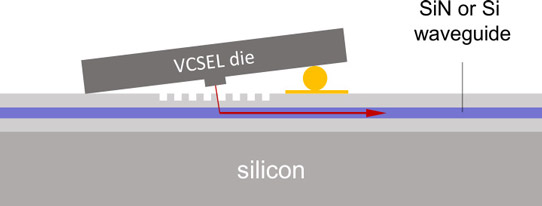
Figure 1: Flip-chip integration of VCSEL die at angle over grating coupler on silicon photonic integrated circuit.
The work is part of the European PIX4life project (https://pix4life.eu/) with the VCSEL providing the light source for a short-wavelength sensor PIC. PIX4life provides a silicon nitride-based photonic integrated platform pilot line for life science and biomedical applications.
The team comments: “The integration technique enables independent optimization of VCSEL performance, eliminates optical feedback to the VCSEL, and facilitates unidirectional coupling without resorting to more complex grating couplers or optical designs needed for normal incidence.”
Grating couplers are polarization sensitive. The team also suggests that many other applications could benefit from its VCSEL’s power, spectral purity, polarization and beam properties.
The VCSEL material was grown on gallium arsenide (GaAs) substrates using metal-organic chemical vapor deposition (MOCVD) – see Figure 2. The active region consisted of indium gallium arsenide (InGaAs) quantum wells in aluminium gallium arsenide (AlGaAs) barriers. The distributed Bragg reflectors (DBRs) were constructed from AlGaAs pairs with different Al content, giving contrasting refractive index values: 29 pairs on the n-side and 21 pairs on the p-side. The interfaces between the different layers of the DBR were graded, and the doping was modulated, in order to reduce electrical resistance and optical losses. The active region was capped with high-Al-content AlGaN, which formed the basis for the oxide aperture that provided lateral optical and electrical confinement.
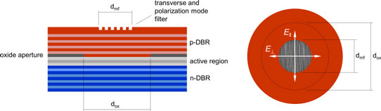
Figure 2: Oxide-confined VCSEL with transverse and polarization mode filter etched into surface. Diameters of oxide aperture (dox) and mode filter (dmf) are indicated and two orthogonal polarization states (E⊥ and E∥) are defined. Left: side view. Right: top view.
The top DBR had a final layer that was a half-wavelength rather than a quarter-wavelength, reducing its reflectively and allowing radiation to exit the device.
Optical simulations were performed to optimize the LP01 E⊥ polarized emission. The calculations suggested values for the oxide aperture and mode-filter diameters of 5μm and 3μm, respectively. The optimum mode filter structure was 120nm and 59nm pitch and depth, respectively.
The grating fill factor was 55% (grating-tooth width/pitch). In fact, the simulations suggested that a fill factor of 80-90% would give the highest polarization-mode selectivity, but the grating fabrication process was higher quality at ~50%. Even so, the selectivity with 55% fill gave 270/cm threshold gain difference.
The VCSELs were fabricated with mesa etching, selective oxidation of the aperture, and contact/pad metalization. The contacts were placed on the top side to enable flip-chip processing onto the PIC system. The mode-filter grating was defined by electron-beam lithography and metal alignment marks, defining both the grating and mesa. The trench depth of the grating was achieved by precise argon ion milling.
The light output was measured with a collimating anti-reflection coated lens between the VCSEL and calibrated large-area detector. The threshold current was 0.4mA. The slope efficiency came in at 1.2W/A. The peak power was 6.5mW before thermal roll-over.
Measurements with a polarizer in the light path showed orthogonal polarization suppression ratios better than 20dB when the current was above 4mA. Spectral analysis gave a 30dB+ suppression factor for higher-order transverse modes at 1mA injection. The 30dB+ trend continued up to 10mA.
The beam profile was found to be near-Gaussian. The 1/e2 full-width was 15° at 2mA and 16° at 10mA. The corresponding full-widths at half-maximum were 9° and 10°. The slight increase in beam width was attributed to thermal lensing effects.
VCSELs Silicon photonic integrated circuits GaAs AlGaAs MOCVD
https://doi.org/10.1364/OE.27.018892
The author Mike Cooke is a freelance technology journalist who has worked in the semiconductor and advanced technology sectors since 1997.


