


- News
14 June 2019
Achieving nitrogen-polar performance from gallium-polar growth
Cornell University in the USA has been using plasma-assisted molecular beam epitaxy (PAMBE) to realize bottom- and top-tunnel junction (TJ) vertical III-nitride blue and green light-emitting diodes (LEDs) [Henryk Turski et al, J. Appl. Phys., vol125, p203104, 2019]. This enabled the team to explore the advantages of reversing the orientation of the charge-polarization-induced electric fields relative to the forward bias direction.
Turski, the lead author, was visiting Cornell from the Institute of High Pressure Physics in Poland, supported partially by the Polish National Centre for Research and Development and the Foundation for Polish Science co-financed by the European Union.
The charge polarization induction of electric fields in III-nitrides arises from the lack of inversion symmetry of the wurtzite crystal structure. Fixed sheet charges arise at heterostructure junctions, giving rise to electric fields of ~1MV/cm. These fields can pull apart electrons and holes, inhibiting recombination into photons (the ‘quantum-confined Stark effect’).
In addition to these problems, the conductivity of n-type III-nitrides tends to be much higher than for p-type material. The gallium nitride substrates used for indium gallium nitride (InGaN) vertical LEDs therefore are n-type in conduction character. Conventional LEDs then have the p-GaN contact at the top of the device (p-side up). The direction of the polarization fields then depends on whether the epitaxy is performed with gallium- or nitrogen-polar growth.
Although it is expected that N-polar LEDs should perform better, growth in that orientation seems to result in material with low internal quantum efficiency (IQE), as found from photoluminescence experiments.
The researchers comment: “The reason for this remains a mystery and is unsolved to date. It is likely related to the difference in defect formation mechanics, e.g. higher layer contamination for growths in the N-polar orientation by metal-organic vapor phase epitaxy (MOVPE) and molecular beam epitaxy (MBE), due to the drastically different growth dynamics and the chemistry of the N-polar and Ga-polar structures.”
The Cornell researchers used tunnel junctions to enable placement of the p-side of the device above or below the active region, avoiding the need for N-polar growth. The tunnel junctions consisted of n- and p-type material.
For effective p-GaN one needs to avoid passivation with hydrogen. For MOVPE growth this is achieved with activation annealing. However, the out-diffusion of hydrogen is blocked when there are overlying layers, restricting devices to top p-GaN contact layers. MBE growth can be arranged to avoid the presence of hydrogen, using nitrogen plasma rather than ammonia (NH3) as precursor, allowing the creation of buried p-type layers.
Another advantage of tunnel junction structures is that the outside contact to metal electrodes can be through thick n-GaN layers, which enable more effective current spreading than p-GaN. Tunnel-junction devices could also realize new geometries for integrating and stacking multiple light emitters. The team also hopes that such “fresh ideas” could eventually lead to lower threshold currents in laser diodes.
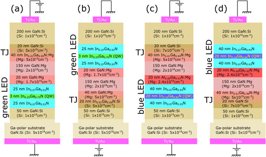
Figure 1: Layer and doping details of quantum well heterostructures with top (a, c) and bottom (b, d) tunnel junctions aimed at blue (c, d) and green (a, b) emission. Researchers referred to structures presented in (a), (b), (c), and (d) as A, B, C, and D, respectively.
The researchers used plasma-assisted molecular beam epitaxy on commercial bulk n-GaN substrates to grow various tunnel-junction/LED combinations (Figure 1). The threading dislocation density of the Ga-polar substrate was ~5x10⁷/cm2. The devices were aimed at blue and green emissions with the tunnel junction variously on top and below the active layers. The GaN layers were grown at 740°C. A lower temperature of 650°C was used for InGaN layers. The ‘quantum wells’ (QWs) in the blue devices were 20nm thick, giving them more the character of double heterostructures. The resulting materials were smooth, with atomic force microscopy (AFM) of 5µmx5µm fields giving roughness values less than 0.5nm.
Fabrication involved device isolation by inductively coupled plasma etch and deposition of titanium/gold electrodes. The bottom electrode consisted of a common contact on the back-side of the substrate. The top electrodes were circular, placed in the center of the mesa. Titanium/gold has a low contact resistance on n-GaN.
The researchers suggest that in future the bottom tunnel-junction contact resistance could be lowered by exploiting a larger cross-section area than for the LED mesa itself. This is not possible for top tunnel-junction devices.
Bottom-TJ devices with 80µmx80µm mesas had higher current flow near the turn-on voltage. This effect was greater in the green-emitters. The researchers say that low leakage levels in all the devices show that the density of extended defects propagating through the LEDs is similar.
The team also suggests that lower tunnel-junction resistance could be achieved by increased doping and polarization-induced effects from InGaN or AlN interlayers. However, such techniques carry the risk of degraded crystal quality in the active region.
The top-TJ LEDs had electroluminescence spectra with two peaks (Figure 2). The high photon energy (shorter wavelength) peak was attributed to parasitic recombination in lower-indium-content layers around the wells. In fact, the parasitic recombination dominated at low current injection levels. The parasitic peaks were not observed for bottom-TJ structures.
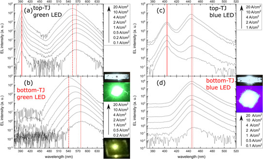
Figure 2: (a)–(d) Electroluminescence spectra in log scale measured on-chip for indicated current densities for 80µmx80µm device. Real-color pictures next to (b) and (d) is whole 1cmx1cm wafer. Above real-color images are monochromatic images collected under microscope for 100µmx500µm Bottom-TJ devices under 100mA injection, showing excellent current spreading.
The bottom-TJ LED also had higher peaks: ~2.5x for green-emission at 20A/cm2, and ~13x for blue. The researchers comment: “The quantitative differences between the enhancement for green and blue emitters can be attributed to differences in active regions and the electron-blocking layer (EBL) design but, irrespective of the details, the bottom-TJ structures for both wavelengths demonstrate the important advantages offered by this conceptual change in the LED design.”
The high-indium-content green LED saw some yellow-to-green shift in the spectral output with increasing injection: from 565nm/580nm for top-/bottom-TJ LEDs to 552nm/541nm, respectively. This was attributed to localized state filling and screening of the internal polarization electric field as injection increased. The researchers see the more pronounced shift in the bottom-TJ device as being evidence of more efficient injection at higher currents. The increased carrier concentration in the quantum well is thought to lead to the higher light output in the bottom-TJ LED.
Simulations of the devices suggested to the researchers that bottom-TJ LEDs suffered less from carrier overshoot effects that can result in efficiency droop at high currents. Overshooting carriers (mostly electrons) recombine non-radiatively in the doped contact layers.
In the presented devices the overshooting carriers could also recombine in the barrier layers, leading to higher-energy photon emission in some cases. The inverted polarization field in the bottom-TJ devices retains the electrons and holes in the quantum well, it is thought. The researchers add: “Because of the separation of electrons and holes outside the QWs, the recombination in the barrier surrounding the QW is significantly reduced for the bottom-TJ LEDs compared to the top-TJ case.”
Capacitance-voltage measurements at 5MHz showed significant hysteresis between up and down sweeps in blue LEDs with top junctions, attributed to charge trapping in the active region. Energy-band simulations suggest that a deep triangular well forms, trapping electrons near the p-side and holes near the n-side of the quantum well. “The hysteresis is caused by charging/discharging of this local, triangular minimum of the potential due to carriers injected or extracted from this region,” the researchers write.
The same triangular structures are also thought to raise barriers to carrier injection into the well at low current, reducing active-region recombination and increasing high-energy photon creation in the cladding layers.
Charge-trapping effects would be detrimental in applications requiring fast modulation, such as is needed for visible light/VLC and ‘light fidelity’/LiFi data communication.
https://doi.org/10.1063/1.5088041
The author Mike Cooke is a freelance technology journalist who has worked in the semiconductor and advanced technology sectors since 1997.


