


- News
6 June 2019
Split gate improves octagonal-cell silicon carbide MOSFET performance
Kijeong Han and B. J. Baliga of North Carolina State University (NCSU) in the USA have combined split-gate structures with their 1.2kV-rated octagonal-cell (OCTFET) layout for 4H-polytype silicon carbide metal-oxide-semiconductor field-effect transistors (MOSFETs) “for the first time” [IEEE Electron Device Letters, published online 17 May 2019].
Han and Baliga reported late last year on the advantages of OCTFET over linear-cell layouts in terms of improved high-frequency figures of merit (HF FOMs) [www.semiconductor-today.com/news_items/2019/feb/ncsu_010219.shtml]. The junction field-effect transistors (JFETs) were designed to operate in accumulation-mode rather than inversion-mode due to higher channel mobility.
The split-gate addition in the latest work removes some gate metal from over the JFET region, decreasing capacitance and charge storage due to reduced gate-to-drain overhang, X (Figure 1). Han and Baliga explain: “The minimization of reverse transfer capacitance (Crss or Cgd) and gate-to-drain charge (Qgd) of the devices is beneficial for improving high-frequency performance because they are dominant factors that determine switching energy loss.”
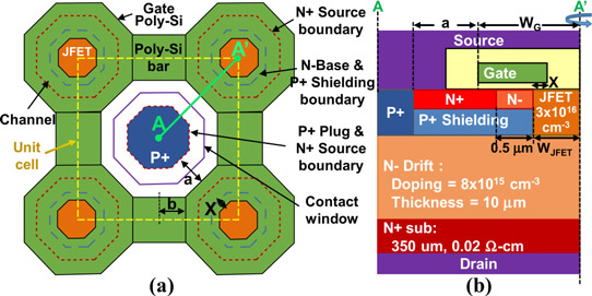
Figure 1: (a) Split-gate OCTFET (SG-OCTFET) cell layout topology. (b) Split-gate MOSFET cell cross-section at A-A’ in SG-OCTFET.
| O_J1.5 | O_J1.1 | O_J1.1_C | O_J1.5_SG | |
| WA-A’ | 5.10μm | 4.53μm | 3.75μm | 5.10μm |
| Channel density | 0.256/μm | 0.259/μm | 0.377/μm | 0.256/μm |
| JFET (X) density | 0.144 | 0.098 | 0.143 | 0.052 |
| Breakdown | 1607V | 1605V | 1605V | 1625V |
| Vth | 2.12V | 2.02V | 2.12V | 2.02V |
| Ron,sp | 8.38mΩ-cm2 | 12.82mΩ-cm2 | 8.47mΩ-cm2 | 8.51mΩ-cm2 |
| Ciss,sp | 32nF/cm2 | 33nF/cm2 | 37nF/cm2 | 33nF/cm2 |
| Coss,sp | 1073pF/cm2 | 1067pF/cm2 | 1069pF/cm2 | 1076pF/cm2 |
| Cgd,sp | 62pF/cm2 | 35pF/cm2 | 48pF/cm2 | 27pF/cm2 |
| Qgd,sp | 233nC/cm2 | 113nC/cm2 | 144nC/cm2 | 88nC/cm2 |
| Ciss/Cgd FOM | 516 | 943 | 771 | 1222 |
| RonxCgd HF-FOM | 520mΩ-pF | 449mΩ-pF | 407mΩ-pF | 230mΩ-pF |
| RonxQgd HF-FOM | 1953mΩ-nC | 1449mΩ-nC | 1220mΩ-nC | 749mΩ-nC |
The devices (were fabricated at a 6-inch SiC power MOSFET foundry run by X-FAB in Texas. The 6-inch 4H-SiC substrate included a 10μm n-SiC epitaxial layer. While the substrate was heavily n-doped, the epitaxial layer was lightly doped to give a drift layer. The gate electrode and MOSFET connecting links consisted of polysilicon (Poly-Si).
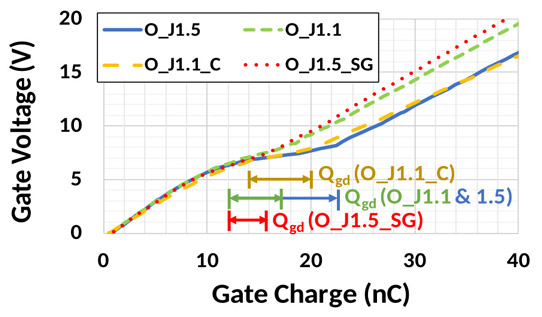
Figure 2: Measured gate charge of fabricated OCTFETs and SG-OCTFET at 800V drain bias and 10A drain current. Active area 0.045cm2.
Simulations were used to optimize the dimensions of the split-gate OCTFET cell: WJFET=1.5μm, a=1.1μm, X=0.3μm. The trade-offs for X included low on-resistance (large X favored) and low capacitance (low X). To keep the peak electric field down, the X value should also avoid the region 0.7-0.9μm, where the expected peak field was of order 4.4MV/cm. For a peak field of less than 4MV/cm, and low HF-FOM values, the X value should be less than 0.3μm.
Table 1: Experimental results for OCTFETs and split-gate OCFET with varying dimensions: O_J1.5, O_J1.1 (a=b=1.1μm), O_J1.1_C (a/2=b=0.55μm), and split-gate O_J1.5_SG. WJFET was either 1.5μm or 1.1μm as indicated in the device code.
The split-gate OCTFET was found to have reduced gate-drain capacitance-charge storage, as represented in the HF-FOMs combining specific on-resistance with gate-drain capacitance and charge storage (RonCgd and RonQgd, respectively, Table 1 and Figure 2). The reduced capacitance/charge compensated for the increased Ron,sp (measured at 20V gate potential, 10A drain current) of the OCTFET layout, relative to linear cells.
Low Cgd also boosted the Ciss/Cgd FOM, where Ciss is the input capacitance, i.e. the sum of Cgd and Cgs. Large values of the Ciss/Cgd FOM are associated with false-turn-on suppression and low shoot-through current when the voltage changes rapidly. The output capacitance, Coss, is the sum of Cds and Cgd.
Han and Baliga also quote the RQ FOM values for Infineon’s silicon-based 600V COOLMOS power transistor (IPL60R365P7) at 1240 (310mΩx4nC), and Cree’s ‘state-of-the-art’ 1.2kV SiC power linear cell topology MOSFET (CREE C2M0160120D) at 2240 (160mΩx14nC). The researchers write: “Our work demonstrates for the first time that a HF-FOM [RonxQgd] 1.66-times better than the 600V COOLMOS product can be achieved in a 1.2kV SiC power MOSFET by using the SG-OCTFET topology, which opens new application opportunities for 1.2kV SiC power MOSFETs.”
https://doi.org/10.1109/LED.2019.2917637
The author Mike Cooke is a freelance technology journalist who has worked in the semiconductor and advanced technology sectors since 1997.


