


- News
27 June 2019
Conductive penetration of aluminium nitride buffers on silicon substrates
Noriko Kurose and Yoshinobu Aoyagi of Ritsumeikan University in Japan claim the first successful fabrication of fully vertical n-type aluminium gallium nitride (n-AlGaN) Schottky diodes on silicon (Si) substrate [J. Appl. Phys., vol125, p205110, 2019]. The device was achieved by creating a conducting path through the normally insulating AlN buffer layer that is needed to grow III-nitride materials on (111)-oriented Si. The conduction was enabled by filling spontaneously formed via holes in the AlN (v-AlN) with n-AlGaN.
Kurose and Aoyagi suggest that the technique could also lead to other vertical high-power devices on silicon, such as vertical n-AlGaN field-effect transistors (FETs), bipolar devices, light-emitting diodes (LEDs), and sensors. Vertical structures push peak electric fields away from the surface of devices where failure often occurs. Production on silicon substrates would substantially reduce manufacturing costs. Further benefit could arise from monolithic integration of III-nitride power structures and silicon control circuitry.
Kurose and Aoyagi used horizontal metal-organic chemical vapor deposition (MOCVD) with trimethyl-gallium (TMG), trimethyl-aluminium (TMA), tetraethyl-silicon (TESi) and ammonia (NH3) precursors in hydrogen carrier gas. The silicon substrates were (111) crystal oriented and doped n-type with antimony.
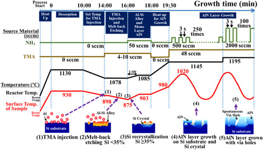
Figure 1: Epitaxial-growth chart and schematic views of cross section of grown layer.
The initial MOCVD growth (Figure 1) generated spontaneous via holes in the AlN nucleation layer. The hole density was (2.5-3.0)x107/cm2, according to optical microscope inspection on samples grown at TMA flow rates of 7 and 8 standard cubic centimeters per minute (sccm). The hole sizes came in the ranges 400-800nm and 500-1000nm, respectively. The depth of the holes were about 80nm, according to atomic force microscopy.
These via holes in the insulating AlN buffer were filled with conductive n-AlGaN using alternate-growth-mode MOCVD where the source materials are fed in in-sequence. The method enhances lateral migration of surface atoms as the growth proceeds.
Scanning electron microscope cross sections of the material showed filling of the via holes with n-AlGaN. Above the via holes. voids tended to form in the overlying n-AlGaN material. A further n-AlGaN layer with somewhat different growth conditions closed the voids and gave a flat surface on which quantum wells and GaN contact layers could be grown.
The voids are seen as being helpful in “reducing the bowing of the epitaxial layer on the Si substrate” and for avoiding cracks in the device layers. Measurements of curvature showed an increase during the AlN growth to 70/km and a decrease to negative values when the n-AlGaN with voids is grown. After cooling, the curvature returned to +70/km. This contrasts with n-AlGaN grown on n-AlN without via holes: the curvature continued increasing to a total of +190/km. This final value was unaffected by cooling.
Vertical conduction structures were made from n-AlGaN layers on v-AlN and non-v-AlN buffers. Ohmic contact metals were applied to both the top n-AlGaN (titanium/aluminium/titanium/gold) and bottom silicon (silver/gold) substrate, followed by sintering. The v-AlN structure demonstrated a low resistance of 33Ω, while the non-v-AlN resistance was 7200Ω. The electrode area was 0.75mm2.
The researchers extracted the specific resistivity of the v-AlN buffer as 100mΩ-cm2, which compares with the non-v-AlN’s 54,000mΩ-cm2.
Schottky diodes were also produced with the n-AlGaN electrode replaced with nickel/gold. The layers between the electrodes consisted of 500μm silicon substrate, 300nm v-AlN, and 1µm n-Al0.3Ga0.7N. The forward/reverse current ratio for +/-20V bias was ~104 (Figure 2). The extracted ideality factor of the Schottky diode was 60 while the barrier height was 0.44eV. The series resistance was estimated to be 900Ω. The forward current density at 20V bias was 4.9A/cm2.
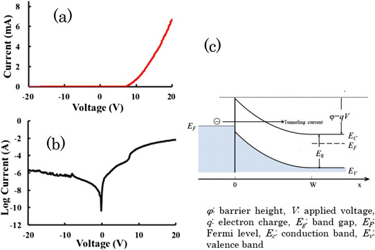
Figure 2: Current-voltage (I–V) characteristics of vertical Schottky diode fabricated on v-AlN: (a) linear plot, (b) logarithmic plot, and (c) band diagram.
The researchers comment: “These values do not indicate a very good Schottky diode performance. This may result from leakage current and/or a high series resistance from our state-of-the-art phase of development of the fully vertical Schottky diode on the Si substrate using v-AlN.”
Comparing the performance of the Schottky and Ohmic devices, the team says that the series resistance mainly originated in the Schottky contact. The thinness of the n-AlGaN layer with unterminated threading dislocations, giving a high leakage current, was blamed for the poor performance. A further effect reducing performance was a high current arising from high fields at the Schottky-electrode edge.
n-AlGaN Vertical Schottky diodes FETs LEDs MOCVD
https://aip.scitation.org/doi/10.1063/1.5058110
The author Mike Cooke is a freelance technology journalist who has worked in the semiconductor and advanced technology sectors since 1997.


