


- News
24 June 2019
TriLumina launches first surface-mount flip-chip back-emitting VCSEL array without need for submount
TriLumina Corp of Albuquerque, NM, USA, which manufactures and integrates flip-chip vertical-cavity surface-emitting laser (VCSEL) array light sources for 3D sensing LiDAR (light detection and ranging) and interior illumination products, has launched the first surface-mount flip-chip back-emitting VCSEL array without the need for a submount or bond wires, allowing lower costs and higher performance than existing designs using near-infrared (NIR) light-emitting laser diodes for 3D sensing.
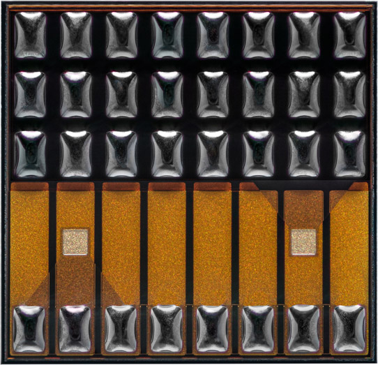
Picture: TriLumina’s 4W chip-on-board SMT VCSEL array.
“For the first time, engineers can create extremely small, low-cost, high-performance products utilizing a NIR surface-mount back-emitting VCSEL array, without the need for a large and costly submount,” says chief marketing officer Luke Smithwick.
Conventional VCSEL arrays are mounted on a submount and use bond wires for electrical connections. TriLumina’s unique, patented flip-chip, back-emitting VCSEL technology has been flip-chip packaged and used in automotive long-range LiDAR prototypes, for low-power mobile, and in-cabin 3D sensing applications. The new 4W chip-on-board (CoB) SMT (surface-mount technology) VCSEL device is a compact, surface-mountable design, consisting of a single VCSEL array die, that is mountable on a printed circuit board (PCB) without the need for a submount carrier for the VCSEL die. This small, very low-cost illumination technology presents a solution for numerous 3D sensing applications, as well as providing innovative NIR illumination options for replacing existing LEDs in applications such as NIR camera systems, mobile cameras, in-cabin occupant monitoring and AR/VR systems. TriLumina’s integrated back-side etched micro-lenses enable integrated optics, which further reduces device height compared with conventional VCSELs with separate optical lenses and can result in lower battery drain with multi-zone operation. It is claimed to have the smallest footprint with the lowest-cost implementation in its class, making it suitable for use in mobile devices.
“TriLumina has led VCSEL illumination for 3D sensing with our innovative flip-chip back-emitting multi-chip illumination modules for long-range LiDAR applications,” claims president & CEO Brian Wong. “Now, we’ve innovated once again, by eliminating the need for a package for low-power mobile and automotive in-cabin applications.”
TriLumina claims that the new architecture has excellent thermal properties with a very compact form factor. The VCSEL has integrated solder balls and mounts directly to a PCB using standard surface-mount technology (SMT), with built-in hermeticity. The CoB SMT VCSEL array eliminates the need for wire bonds or other expensive packaging technology found on standard top-emitting VCSELs. Although the device is designed for efficient operation in indirect time-of-flight (ToF) applications, the lack of wire bonds also has inherently low parasitic inductance, making the emitter compatible with ultra-high-resolution, fast rise-time, short pulse-width direct ToF applications.
TriLumina and Analog Devices collaborate on illuminator module for automotive Flash LiDAR
DENSO invests in laser technology startup TriLumina


