


- News
4 March 2019
G-ray Nanotech and IKZ collaborate to develop detector-grade GaAs wafers
G-ray Nanotech (part of development-stage company G-ray Industries SA of Neuchâtel, Switzerland) and IKZ (Leibniz Institute for Crystal Growth) in Berlin, Germany have entered into a long-term R&D collaboration covering the doping of gallium arsenide (GaAs) structures and the manufacturing of high-purity crystals in wafer form factor for detector applications.
“The competencies of IKZ will allow us to accelerate significantly the expansion of our latenium detector architecture into medium-large energy x-rays applications as well as in the infra-red spectrum,” says G-ray Nanotech’s CEO Philippe Le Corre.
G-ray Industries SA is developing ultra-high-performance detectors dedicated to industrial non-destructive-testing solutions. Based on G-ray’s patented latenium technology, the detectors are being developed in partnership with Switzerland’s Center for Electronics and Microtechnology CSEM (Centre Suisse d’Electronique et de Microtechnique).
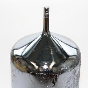 Picture: 4-inch gallium arsenide single crystal, grown by VGF method. (Courtesy of Matthias Kern, IKZ.)
The latenium evaluation kits are available for evaluation purposes from first-quarter 2019. Also, G-ray’s technologies - in particular the covalent bonding of a silicon wafer to a GaAs, germanium or silicon wafer at low temperatures and the very fast epitaxial growth of germanium structures - are being targeted at the fields of high-energy physics research for new particle detectors and at vision systems for the automotive industry.
“IKZ is committed to push high-performance crystalline materials to market applications, and the state-of-the-art x-ray imaging detector development at G-Ray is a nice opportunity for us,” comments IKZ’s scientific director professor Thomas Schroeder. “We consider 3D heterointegration via bonding approaches as a fruitful strategy for us to innovate technologies by high-quality, precisely tailored crystalline materials,” he adds.
“With our expertise in materials science and technology we have supported the G-ray team right from the start,” says Gian-Luca Bona, CEO of Empa (the Swiss Federal Laboratories for Material Science and Technology). “This is an outstanding opportunity to bring a ground-breaking x-ray detector technology to the market.”


