


- News
19 March 2019
Indium gallium arsenide quantum well transistors on silicon
IBM Research Zürich in Switzerland claims the highest combined values of high-frequency cut-off for radio frequency (RF) III-V metal-oxide semiconductor field-effect transistors (MOSFETs) on silicon (Si) [Cezar B. Zota et al, IEEE Electron Device Letters, published online 1 March 2019]. The team further reports that their device outperforms state-of-the-art silicon RF-CMOS.
The researcher used an indium gallium arsenide (InGaAs) quantum well (QW) channel defined by indium phosphide (InP) barriers that “reduced the impact of border traps on the transconductance within the measured frequency range”.
The QW channel material was integrated on silicon on buried oxide (BOX) using direct wafer bonding. The silicon-on-oxide layer was not intentionally doped. The well consisted of 10nm In0.75Ga0.25As sandwiched between InP barrier layers (20nm bottom, 2nm top).
The replacement metal gate fabrication process began with deposition of an amorphous silicon dummy gate. Silicon nitride was used for source/drain spacing. The spacer formation was achieved using a combination of atomic layer deposition (ALD) and reactive ion etch.
Contact extensions beneath the spacers ensured reduced parasitic overlap capacitance and access resistance. The cavities for the contact extensions were formed by ‘digital’ cycles of controlled oxidation and etching. The digital etch also removed the top InP barrier from the source/drain contact regions. The contact extension cavities were filled with n-InGaAs via metal-organic chemical vapor deposition (MOCVD).
The dummy gate was then removed and replaced with aluminium oxide and hafnium dioxide high-k gate insulator, and titanium nitride and tungsten gate metal layers (Figure 1).
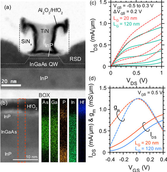
Figure 1: (a) Cross-sectional scanning transmission electron micrograph (STEM) image of 20nm gate-length device before M1-interconnect metallization. (b) High-resolution TEM of channel heterostructure together with energy-dispersive x-ray spectroscopy map of highlighted region. (c) Output characteristics of 20nm and 120nm devices, respectively. (d) Transfer characteristics of same devices.
The output conductance of a 20nm gate-length MOSFET was 50% higher than reference devices without the top InP barrier. The peak transconductance occurred at 0V gate potential – a desirable feature for RF operation due to gate oxide reliability considerations. The presence of the top barrier eliminates defect scattering at the semiconductor/gate oxide interface.
The peak transconductance was 1.25mS/μm for 20nm and 120nm gate MOSFETs. The constancy of the transconductance with gate length scaling was attributed to short-channel effects. The highest peak transconductance measured for devices with gate lengths in the range 20-120nm was 1.4mS/μm (2.1mS/μm intrinsic). The team suggests that gate oxide scaling and process optimization could push this up.
By contrast, transconductance increased with decreased gate length in the reference devices without the top barrier. Devices without any barriers had similar behavior to the reference MOSFETs without the top barrier.
The peak transconductance of the QW MOSFET was 300% greater than that of the reference devices when the gate length was 120nm. The improvement decreased to 60% at the short gate length of 20nm.
The effective mobility of the QW channel was 1500cm2/V-s, compared with 500cm2/V-s for the channel without the top InP barrier. The researchers comment: “This difference is attributed to reduced oxide interface traps and surface roughness scattering using the QW.”
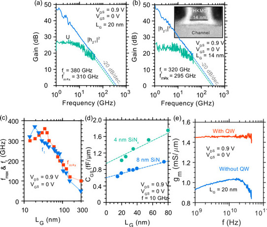
Figure 2: (a) Gain plot of 20nm device under optimal biasing conditions. (b) Gain plot of 14nm device, with inset showing STEM image of device cross-section. (c) Simultaneous ft and fmax versus gate length (LG). (d) Gate-to-source capacitance for devices with 4nm and 8nm thick spacers, respectively. (e) Transconductance frequency dependence with and without quantum well.
Frequency-dependent measurements were carried out between 1GHz and 45GHz (Figure 2). The cut-off frequency (ft) for a 20nm gate-length MOSFET was 370GHz and the maximum oscillation (fmax) was 310GHz. The device had two 4μm-wide gate fingers branching off from a central stem. The team reports that these values “represent the highest combined ft and fmax reported for a III-V MOSFET on silicon”. An even higher fmax of 360GHz was achieved with 35nm gate length.
https://ieeexplore.ieee.org/document/8656532
The author Mike Cooke is a freelance technology journalist who has worked in the semiconductor and advanced technology sectors since 1997.


