


- News
19 March 2019
Eliminating waveguide propagation from III-nitride light-emitting diodes
Nanjing University of Posts and Telecommunications in China have been experimenting with ultrathin vertical III-nitride light-emitting diodes (LEDs) with a view to enhancing light extraction [Yongjin Wang et al, Appl. Phys. Express, online 12 February 2019].
Thicker III-nitride LEDs tend to trap emitted light into in-plane waveguide mode propagation due to the large refractive index of gallium nitride (GaN) compared with air. The contrast in refractive index narrows the escape cone, meaning light can be trapped by severe-to-total internal reflections at the air/semiconductor interfaces. Thinning the LED should eliminate waveguide modes, forcing light out of the structure.
The transferred thin-film epitaxial material comprised 2200nm of n-AlGaN, 108nm of multiple quantum wells, and 90nm of p-GaN. The material was bonded p-side down on a 2-inch conductive silicon wafer (Figure 1). The metal bonding layers consisted of a nickel/silver p-electrode/reflector and nickel/tin adhesion layers.
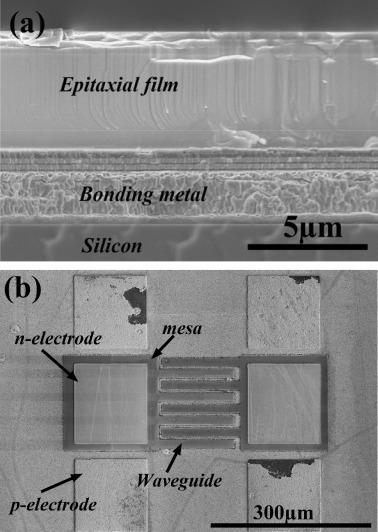
Figure 1: (a) Cross-sectional scanning electron microscope (SEM) image of III-nitride epitaxial films. (b) Plan-view SEM image of fabricated LEDs.
The bonded structure was then subjected to inductively coupled plasma etch to reduce the film thickness to around 225nm. Selective etching down to the silver metal with masked areas was then used to define device mesas. More masking was used to create nickel/gold p- and n-electrodes.
The researchers arranged 4 18μmx155μm waveguides on the wafer to enable the assessment of in-plane propagation of emitted radiation. The LEDs could also act as photodiode (PD) detectors. Some of the LEDs were arranged 12μm away from the end of the waveguide end-facet as photodiode monitors.
The dominant output peak wavelength varied between 413.8nm and 411.8nm, respectively, as the forward voltage increased from 3.4V to 4.2V. These wavelengths are in the visible violet range of 380-450nm.
Reflectance measurements on LEDs with 225nm and 1430nm epitaxial layers suggested that the reflectivity of the nickel/silver mirror electrode was greater than 85% over a wide angle range.
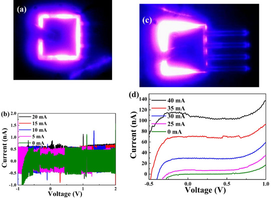
Figure 2: (a) Light emission image of 225nm-thick LED. (b) Measured current (mostly noise) of photodiode as function of LED injection current. (c) Light emission from 1430nm-thick LED. (d) Measured photocurrent of 1430nm structure.
The use of a thin epitaxial layer of 225nm thickness eliminated waveguide modes and enhanced light extraction. Comparison between 225nm- and 1430nm-thick LEDs showed a lack of light emanating from the end facets of the waveguides in the former device (Figure 2), unlike in the thicker construction.
https://iopscience.iop.org/article/10.7567/1882-0786/ab0664
The author Mike Cooke is a freelance technology journalist who has worked in the semiconductor and advanced technology sectors since 1997.


