


- News
9 May 2019
Graphene interlayer for deep ultraviolet LEDs on nano-patterned sapphire
Researchers based in Beijing, China, have used graphene (Gr) to improve aluminium nitride growth on nano-patterned sapphire substrates (NPSSs) as a template for aluminium gallium nitride (AlGaN) deep ultraviolet (DUV) light-emitting diodes (LEDs) [Hongliang Chang et al, Appl. Phys. Lett., vol114, p091107, 2019].
The team was variously based at Research and Development Center for Semiconductor Lighting Technology, University of Chinese Academy of Sciences, Peking University, and State Key Laboratory of Superlattices and Microstructures.
The presence of graphene improved aluminium mobility on the growth surface, improving crystal quality through quasi-van der Waals epitaxy (QvdWE). In turn, this improved the performance of an AlGaN LED grown on the AlN template.
DUV LEDs are desired for a range of uses such as sterilization, polymer curing, biochemical detection, non-line-of-sight communication and special lighting. However, the efficiency of LEDs in the 200-300nm wavelength range is low (of the order a few percent). Sapphire is the preferred substrate, but suffers from lattice and thermal expansion mismatches with AlN that introduces strain/stress, generating efficiency-killing defects.
The nano-patterned sapphire substrate consisted of 400nm-deep nano-concave cone patterns with 1μm period produced by nano-imprint lithography (NIL) on the sapphire surface. The unetched regions were 300nm wide. The ~0.7nm-thick graphene layer was grown by 1050°C catalyst-free atmospheric pressure chemical vapor deposition (APCVD). The graphene growth process took three hours. The precursor was methane in hydrogen/argon carrier.
The graphene was subjected to reactive ion etch to introduce defects that would increase chemical reactivity with the subsequent AlN growth. Without defects, AlN does not attach easily to graphene, slowing AlN growth.
The graphene on NPSS was prepared with 30-second exposure to nitrogen plasma before loading into the metal-organic chemical vapor deposition (MOCVD) reactor for AlN growth. Raman spectroscopy suggested that the nitrogen plasma treatment generated increased numbers of dangling bonds.
The 1200°C AlN growth used trimethyl-aluminium and ammonia precursors in hydrogen carrier gas. There was no low-temperature nucleation step. The full growth time was two hours. Some samples were grown for just 10 minutes to allow study of the initiation of AlN deposition.
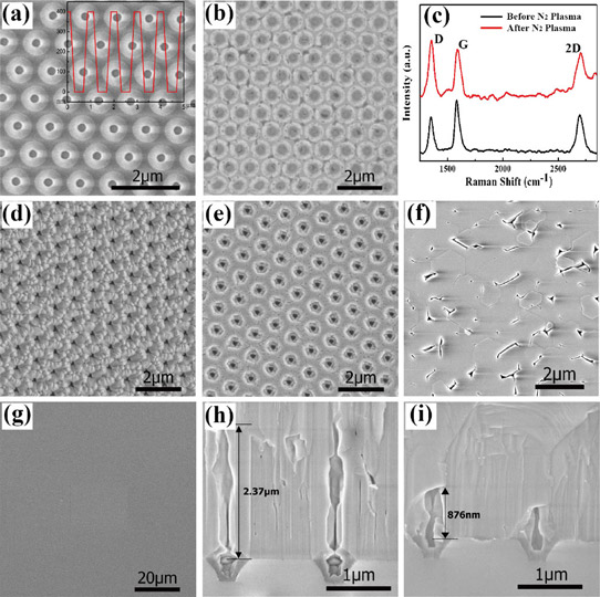
Figure 1: (a) SEM image of bare NPSS. Inset in (a) shows line profile from atomic force microscopy. (b) SEM image of as-grown graphene films on NPSS. (c) Raman spectra of graphene film before (black) and after (red) nitrogen plasma treatment. (d) and (f) SEM images of initial 10 minutes and 2 hours growth of AlN films on NPSS without graphene interlayer. (e) and (g) SEM images of initial 10 minutes and 2 hours growth of AlN films on NPSS with graphene interlayer. (h) and (i) cross-sectional SEM images of AlN films on NPSS without and with graphene interlayer.
Without a graphene interlayer, two hours of growth on NPSS resulted in rough, non-uniform AlN layers (Figure 1). By contrast, the graphene interlayer enabled rapid coalescence of the AlN, giving a continuous, flat surface. Cross-sectional scanning electron microscopy (SEM) showed that the coalescence occurred within 1μm of the full ~2.4μm growth.
X-ray rocking-curve analysis showed a reduction in the full-width at half maximum (FWHM) of the peak associated with the (0002) plane of the AlN lattice from 455.4arcsec to 267.2arcsec, arising from the graphene interlayer. The (10-12) peak FWHM also decreased from 689.2arcsec to 503.4arcsec. These values resulted in respective estimates for screw and edge dislocations: 4.51x10⁸/cm2 and 4.40x10⁹/cm2 without graphene interlayer, reducing to 1.55x10⁸/cm2 and 2.60x10⁹/cm2 with graphene.
According to Raman spectroscopy, the biaxial stress was reduced from 0.87GPa to 0.25GPa by the use of graphene interlayers.
Simulations of the growth process suggested that the effect of the graphene layer was to increase the mobility of aluminium adatoms, compared with the bare NPSS surface. The researchers comment: “The strong binding of Al adatoms to the defect sites and the free diffusion on the non-defective regions ensure the effective nucleation and fast growth for AlN layers, as observed in our experiments.”
The AlN on bare NPSS undergoes “three-dimensional longitudinal island growth” due to the sluggish diffusion of the Al adatoms. The coalescence of the islands is therefore delayed. On graphene, the Al adatoms can diffuse further in shorter time, allowing “lateral two-dimensional growth” with rapid lateral coalescence.
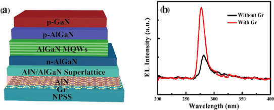
Figure 2: (a) Schematic diagram of AlGaN-based DUV-LED. (b) Electroluminescence spectra with and without graphene interlayer.
The researchers used the AlN/Gr/NPSS template to produce a deep ultraviolet LED (Figure 2). The epitaxial structure consisted of a 1130°C 20-period 2nm/2nm AlN/Al0.6Ga0.4N superlattice, 1.8μm n-Al0.55Ga0.45N contact, 5-period 3nm/12nm Al0.4Ga0.6/Al0.5Ga0.5N multiple quantum well (MQW), 50nm p-Al0.65Ga0.35N electron-blocking layer (EBL), a 30nm p-Al0.5Ga0.5N cladding layer and a 150nm p-GaN contact layer. Post-growth annealing was used to activate the p-type layers (800°C for 20 minutes in nitrogen).
At 40mA, the 280nm-wavelength peak was around 2.6x higher than that for electroluminescence from an LED grown on bare NPSS. The researchers attribute the higher intensity to a reduced defect density in the graphene-based sample.
Deep Ultraviolet LEDs Nano-patterned sapphire Graphene AlN AlGaN
https://doi.org/10.1063/1.5081112
The author Mike Cooke is a freelance technology journalist who has worked in the semiconductor and advanced technology sectors since 1997.


