


- News
10 May 2019
Positive threshold in GaN transistors with p-type aluminium titanium oxide
The Indian Institute of Science claims the first enhancement-mode (e-mode) operation of aluminium gallium nitride/gallium nitride (AlGaN/GaN) high-electron-mobility transistors (HEMTs) using p-type aluminium titanium oxide (AlTiO) gate insulation [Sayak Dutta Gupta et al, IEEE Transactions on Electron Devices, published online 16 April 2019].
The metal-oxide-semiconductor (MOS) gate stack combined the high-k dielectric properties of TiO2 (k greater than 60) with the p-type properties supplied by Al2O3 doping (k ~9). The Al2O3 substitutes the 2Als on Ti sites and the 3Os have a deficit of one vacancy that is doubly positively charged. The charged O vacancy can release two holes, which can subsequently be reabsorbed by uncharged O vacancies. The compensating negative charges on the 2 Al sites are fixed.
The researchers comment: “The ON-state performance of e-mode HEMTs in this paper with p-type AlTiO was found to be on par with the best reports till date.”
GaN HEMTs are being developed as power switches, where enhancement-mode as opposed to depletion-mode is desired for low power loss and fail-safe performance. Enhancement-mode devices are in the low-current OFF-state when the gate potential is at 0V. By contrast, depletion-mode operation has the current on with 0V gates and requires a (negative) potential to pinch off the electron flow.
Unfortunately, simple GaN HEMTs are depletion-mode and special extra processing is required to push threshold voltages in a positive direction to give enhancement-mode, normally off performance. The placing of p-type materials, such as magnesium-doped p-GaN, under the gate is one such method for moving to enhancement-mode devices. Recessing the gate into the barrier also pushes the threshold positive, but removing all the barrier material increases on-resistance due to etch damage of the GaN channel surface.
High-k dielectrics give increased electrostatic control of current under the gate with sharper turn-on (low subthreshold swing), while reducing gate leakage, compared with Schottky gate HEMTs.
Metal-organic chemical vapor deposition (MOCVD) on 6-inch (111) silicon substrates produced epitaxial structures with 150nm AlN nucleation, 1μm AlGaN transition, 3μm GaN buffer/channel, 22nm Al0.22Ga0.78N barrier, and 40nm in situ silicon nitride cap.
Fabricated transistors (Figure 1) consisted of annealed titanium/aluminium/nickel/gold source-drain contacts, plasma-etched mesa isolation, atomic layer etching (ALE) of the AlGaN barrier for gate recessing, surface treatment and deposition of gate oxide, and nickel/gold gate metal formation and low-temperature annealing.
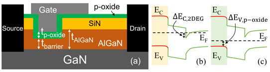
Figure 1: (a) Cross-sectional view of HEMT with p-type metal oxide gate and partially recessed AlGaN barrier. Energy-band sketch of AlGaN/GaN HEMTs with (b) conventional dielectric and (c) p-type oxide: p-type oxide shifts Fermi level (EF) beneath conduction band (EC) in two-dimensional electron gas (2DEG) channel.
The gate oxide was applied using BENEQ atomic layer deposition (ALD) equipment. Water (H2O) was used as precursor for oxygen in both the TiO2 and Al2O3 components. The titanium was sourced from titanium tetraisopropoxide (TTIP), and aluminium from trimethylaluminium (TMA). The oxide was built up from cycles of Al2O3 and TiO2 layers.
Hall measurements on Al0.52T0.48O showed p-type conductivity with a majority hole concentration at 1.4x10¹⁴/cm3. The Al0.52T0.48O material was compared as a p-type gate oxide against MOS-HEMT structures incorporating pure TiO2, sputtered copper oxide or electron-beam evaporated nickel oxide.
Pure TiO2 gate insulation resulted in depletion-mode operation with a threshold voltage at -4V. With 52% Al in the TiO2, the threshold shifted in a positive direction to -0.2V. Post-deposition annealing also pushed the threshold positively as the temperature increased, but the effect became less pronounced for higher Al contents of the AlTiO. The more positive effect at lower contents is due to greater activation of the Al, it is thought. At 52% Al, the number of Ti sites where Al can be activated is limited.
Copper oxide gave a smaller threshold shift than AlTiO. In addition, the gate leakage was increased by up to four orders of magnitude. With nickel oxide, the gate leakage was even worse.
Thinning the barrier by recessing the gate enabled positive threshold voltages to be attained. With the barrier thickness at 8nm, the threshold was +0.5V. The resulting transistor operated in enhancement-mode with the device in the OFF-state at 0V gate potential. The thinner barrier also improved channel control with lower OFF-state current (100x lower) and improved/lower subthreshold swing at 73mV/decade (Figure 2).
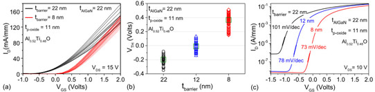
Figure 2: (a) Transfer characteristics of HEMTs with optimized p-oxide and different barrier thicknesses. (b) Shift in threshold (VTH) from negative to positive when barrier thickness under the gate was scaled. (c) Logarithmic plot of transfer characteristics and derived subthreshold swing (SS) values.
The threshold voltage hysteresis for drain current-gate voltage dual sweeps was ~30mV and ~40mV with the drain bias at 0.1V and 15V, respectively.
A device with 3μm gate length and 17.5μm source-drain spacing achieved a drain current ~400mA/mm at +4V gate potential. The on-resistance was 8.9Ω-mm, while the on/off current ratio was 107. Gate leakage was less than 200nA/mm.
The OFF-state three-terminal breakdown voltage was more than 600V with the substrate grounded. Catastrophic failure was seen in the mesa isolation, not as usual in the gate-drain region. The researchers expect an increased breakdown voltage from improved mesa isolation processes.
The researchers believe that the threshold can be pushed beyond +1V with optimization of the p-oxide gate insulation.
AlTiO gate insulator GaN GaN HEMTs
https://doi.org/10.1109/TED.2019.2908960
The author Mike Cooke is a freelance technology journalist who has worked in the semiconductor and advanced technology sectors since 1997.


