


- News
2 May 2019
Diamond thermal management boosts gallium nitride transistor power
A team of researchers mainly based at the US Naval Research Laboratory (NRL) claim record DC power density from aluminium gallium nitride (AlGaN) barrier high-electron-mobility transistors (HEMTs) [Marko J. Tadjer et al, IEEE Electron Device Letters, published online 11 April 2019]. Other researchers in the team were variously from Southern Methodist University, TMX Scientific, University of California Los Angeles (UCLA) and Akash Systems Inc in the USA.
The high power was achieved by replacing the silicon substrate on which the III-nitride device layers were grown with diamond to allow enhanced thermal management.
The team targets the high frequency and high power density needed for commercial and military electronics. Diamond has previously been used to manage the high temperatures generated in such applications, due to its very high thermal conductivity. One technique for this is wafer bonding, but an attractive alternative is to grow diamond directly on the backside of the device layers.
Building on previous work, the NRL-led team inverted the GaN/Si substrate and removed the silicon substrate. Etching of the exposed N-polar III-N nucleation layers left some 700nm of GaN buffer. A 30nm silicon nitride (SiN) barrier was applied before chemical vapor deposition (CVD) of a thick polycrystalline diamond layer at Element Six Technologies (E6, part of the De Beers Group).
E6 specializes in synthetic diamond and tungsten carbide growth processes. In addition to thermal management, applications for these ‘supermaterials’ cover sectors such as oil and gas extraction, automotive and aerospace parts, mining and construction, consumer electronics, optics, and wear reduction in mechanical systems. The company claims employment of 1900 people with production facilities in UK, Ireland, Germany, South Africa and the USA. E6 traces its history back to 1946.
The NRL device structure was completed with a 20nm Al0.2Ga0.8N barrier layer, mesa plasma etch, titanium/aluminium/nickel/gold ohmic source-drain contact deposition and annealing, nickel/gold Schottky gate deposition, titanium/gold contact pad overlay, and plasma-enhanced chemical vapor deposition (PECVD) silicon nitride passivation. The device fabrication was carried out both before and after the silicon substrate replacement with diamond. The silicon nitride passivation was optimized for avoiding current collapse under pulsed operation.
The researchers report: “Room-temperature Hall measurements and DC current-voltage characteristics indicated that the substrate-side process did not significantly influence the mobility and sheet carrier density, and thus the on-resistance of the HEMTs. Additionally, only minimal effects on threshold voltage and transconductance were observed.”
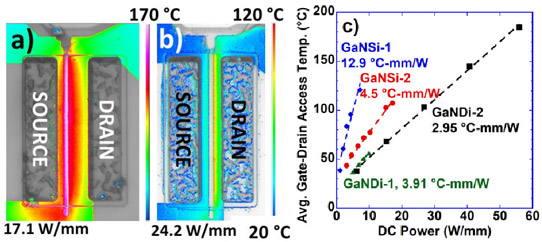
Figure 1: Steady-state thermoreflectance maps of AlGaN/GaN HEMTs before and after backside diamond deposition process measured at 365nm illumination as function of DC output power: (a) silicon-based sample GaNSi-2; (b) diamond-based ample GaNDi-2; and (c) average temperature in gate-drain access region as function of DC power (IDS xVDS) for range of AlGaN/GaN HEMTs.
Thermoreflectance imaging (TRI) showed temperature increases near contacts beyond 150°C under 15W/mm power density direct current (DC) operation of HEMTs on silicon (Figure 1). By contrast, the device on diamond demonstrated no significant temperature increase with 24.2W/mm power density. Above 24.2W/mm, the temperature did increase, largely due to gate leakage current. Even so, the temperature did not exceed 176°C in the access/contact region with the power density at 56W/mm. The maximum temperature of 205°C was seen in the gate region at the drain edge.
The diamond-based GaN HEMT (GaNDi-2) achieved a thermal resistance as low as 2.95°C-mm/W. A device from an earlier version of the diamond replacement (GanDi-1) process had a higher thermal resistance of 3.91°C-mm/W. The higher value was attributed to defects at the interface with the diamond substrate. Transmission electron micrography (TEM) showed nanometer-sized voids in the GaNDi-1 sample’s 30nm silicon nitride layer and at the GaN interface (Figure 2). The GaNDi-2 sample, by contrast, achieved “a sharp GaN-diamond interface and lower thermal resistance”. The thermal resistance was significantly higher for GaN HEMTs on the original silicon substrates (GaNSi-1&2).
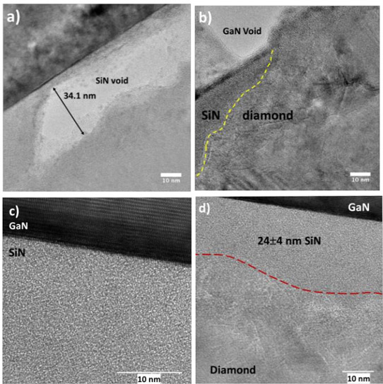
Figure 2: High-resolution TEM image of GaN/SiN/diamond interface of (a) sample GaNDi-1 showing void in SiN, (b) sample GaNDi-1 showing void in N-polar side of GaN caused by H-plasma etching during diamond CVD, (c) sharp, void-free interface between amorphous SiN and crystalline GaN for sample GaNDi-2, and (d) SiN/polycrystalline diamond substrate interface for sample GaNDi-2 (delineated by dashed red line).
The researchers suggest that thinning or eliminating the silicon nitride barrier layer could decrease the thermal resistance by up to 48%. However, such a process would need also eliminate voids from the interface.
AlGaN barrier HEMTs AlGaN PECVD
https://doi.org/10.1109/LED.2019.2909289
The author Mike Cooke is a freelance technology journalist who has worked in the semiconductor and advanced technology sectors since 1997.


