


- News
30 May 2019
Nitrogen-polar gallium nitride current-aperture vertical electron transistor
Researchers based in the USA have reported the ‘first demonstration’ of a nitrogen-polar (N-polar) gallium nitride (GaN) current-aperture vertical electron transistor (CAVET) [Saba Rajabi et al, IEEE Electron Device Letters, published online 1 May 2019]. The device also achieved a blocking electric field of 2.9MV/cm.
The use of N-polar structures allows the use of an aluminium gallium nitride (AlGaN) back-barrier to induce a two-dimensional electron gas (2DEG) in an overlying GaN channel layer. This reverses the usual structure in Ga-polar material where a top AlGaN barrier layer is used. A back-barrier structure is attractive in radio-frequency power applications such as amplifiers to reduce power losses. Another attractive feature is that Ohmic metal contact is not impeded in the presence of a top barrier.
CAVETs combine a lateral channel and a vertical voltage-blocking structure that allows higher electric fields and eliminates dispersion/current collapse under pulsed operation.
University of California Davis (UCD), University of California Santa Barbara (UCSB) and Stanford University used metal-organic chemical vapor deposition (MOCVD) epitaxial growth on c-plane sapphire, beginning with an unintentionally doped (UID) GaN buffer layer. The structure (Figure 1) continued with 200nm n+-GaN drain and 200nm UID n-GaN drift layers.
The current-block layer (CBL) regions were formed using selective-area implantation of magnesium ions (Mg2+) into the drift layer. The implantation was followed by annealing at 1280°C for 30s in nitrogen atmosphere.
According to the researchers, the annealing did not need a cap layer due to the thermal stability of the N-polar GaN. Such cap layers can have detrimental effects since they can crystallize, making removal difficult. “This is another advantage of N-polar GaN that can play a very important role in implantation-based device technology,” the researchers write.
After the implantation, further layers were grown at 1160°C: 3nm graded AlGaN, 1nm AlN, 150nm n-GaN, and 40nm n+-GaN. Secondary-ion mass spectrometry (SIMS) showed that the AlN barrier was effective in blocking out-diffusion of Mg atoms from the CBL into the regrown layers. Such out-diffusion would negatively impact the 2DEG region that forms near the AlN/n-GaN interface in the regrown structure.
Fabrication began with chlorine-based inductively coupled plasma (ICP) etch of isolation 400nm-high mesas. Reactive-ion etch (RIE) exposed the gate and access regions of the transistor. The gate dielectric and surface passivation consisted of 20nm of MOCVD silicon nitride.
The ohmic contact regions were exposed with fluorine-based RIE through the silicon nitride. The source/drain ohmic contact metal stacks were annealed titanium/aluminium/nickel/gold. The gate metal was nickel/gold.
The gate electrode was split in two to minimize gate-drain leakage and to maximize electrostatic control over the source current. The gate length (Lg) and width were 566nm and 150μm, respectively. The gate-source (Lgs) distance was 2μm; the gate-aperture (Lga) distance was 1.3μm. The aperture gap (Lap) was 2μm.
With the gate at 0V, the maximum drain current density was 1.68kA/cm2; the specific on-resistance was 2.48mΩ-cm2. The current density and specific on-resistance were normalized according to the source contact lengths and source-source distance (11.3μm) and the device width (150μm), giving an area of 1.7x10⁻⁵cm2. The current pinched-off when the gate was at -8V. The on/off current ratio was 106.
Pulsed measurements showed no dispersion from DC performance. The team attributed this to the vertical structure whereby the peak electric field is situated deep the drift region, away from the surface traps that impact pulsed performance.
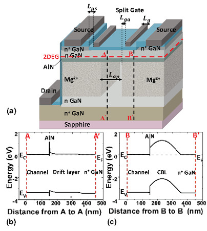
Figure 1: (a) Sketch of N-polar AlN/GaN-based CAVET. (b,c) Band diagrams through aperture (A-A’) and CBL (B-B’) regions, respectively.
With the gate pinched-off, the breakdown voltage (Figure 1) was 58V for a leakage of 1mA/cm2. The researchers estimate the peak electric field at 2.9MV/cm. The researchers claim this as the “first evidence of such a high breakdown field achieved in vertical N-polar GaN transistors.”
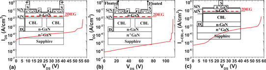
Figure 2: Three-terminal breakdown with the gate at pinch-off (-8V). (b) Gate dielectric breakdown test with floating source. (c) n-CBL-n test structure measurement.
Experiments on various test structures indicated that the breakdown occurred via punch-through in the current-block layer, not the gate dielectric. The team believes that the CBL could be improved with a more uniform, thicker implantation profile. Thicker, lower-doped drift regions also would enable increased breakdown voltages. The researchers say that there is progress towards growing such thicker drift regions on N-polar GaN with lower dislocation density generation, as needed for high breakdown voltages and low leakage.
N-polar GaN GaN AlGaN CAVET MOCVD
https://doi.org/10.1109/LED.2019.2914026
The author Mike Cooke is a freelance technology journalist who has worked in the semiconductor and advanced technology sectors since 1997.


