- News
28 November 2019
Electrochemical membrane release for aluminium gallium nitride devices
Researchers in Sweden and Germany have been developing electrochemical etching as a means to create thin-film aluminium gallium nitride (AlGaN) optoelectronic and power-electronic devices [Michael A. Bergmann et al, Appl. Phys. Lett., vol115, p182103 2019]. AlGaN alloys are wide-bandgap materials with the potential for deep ultraviolet (UV) light emission and for electronics that can sustain high electric fields and voltages before breakdown.
The researchers at Sweden’s Chalmers University of Technology, Germany’s Technische Universität Berlin and Sweden’s KTH Royal Institute of Technology comment: “Heterogeneously integrated AlGaN epitaxial layers will be essential for future optical and electrical devices like thin-film flip-chip ultraviolet light-emitting diodes, UV vertical-cavity surface-emitting lasers, and high-electron-mobility transistors on efficient heat sinks. Such AlGaN membranes will also enable flexible and micromechanical devices.”
Releasing the AlGaN layers from the epitaxial growth substrate would enable vertical cavities with dielectric applied to both sides of a membrane. For high-power electronics, thin-film formats would allow better thermal management by applying the active semiconductor layers directly to heatsinks. However, present methods for releasing AlGaN such as laser lift-off tend to damage the material, reducing performance in the final device.

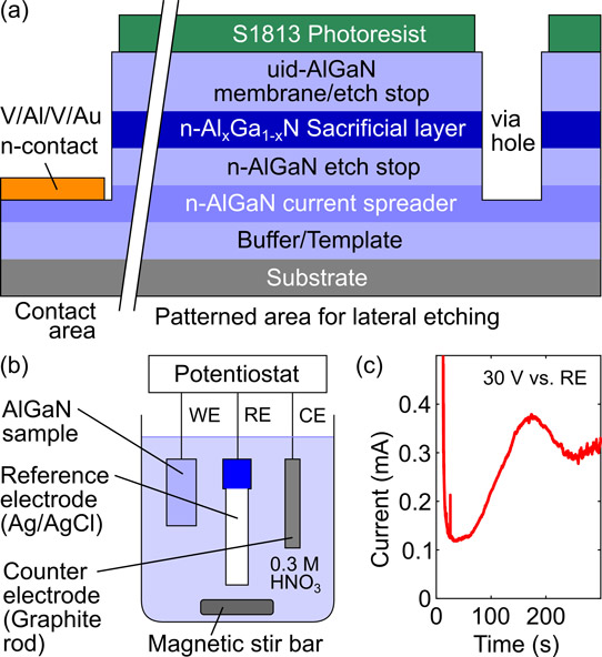
Figure 1: (a) AlGaN sample structure, (b) three-electrode setup for electrochemical etching, and (c) etching current versus time for etching Al0.11Ga0.89N sacrificial layer at 30V.
The researchers first grew a 2x10¹⁸/cm3 silicon-doped Al0.5Ga0.5N layer on c-plane sapphire with an AlN template layer using a close-coupled showerhead metal-organic chemical vapor deposition (MOCVD) reactor (Figure 1). The n-type conductivity from the silicon doping ensured current spreading for uniform electrochemical etching.
The current-spreading layer was followed by a 225nm 0.5x10¹⁸/cm3 {Si] lightly doped Al0.5Ga0.5N etch-stop layer. The sacrificial layer for membrane release was 130nm 2x10¹⁹/cm3 heavily Si-doped AlxGa1-xN. The membrane layer was 580nm (1900nm for Al0.11Ga0.89N sacrificial layer sample) unintentionally doped Al0.5Ga0.5N.
X-ray analysis showed that the Al0.5Ga0.5:Si was ‘pseudomorphic’ - i.e. strained – on all sacrificial layer compositions.
The electrochemical etching was enabled by dry reactive-ion etching 10μm-diameter via holes in a 7x9 400μm pitch array to expose the sacrificial layer. The etched holes reached down to the current-spreading layer. The electrochemical contact with the current-spreading layer was made through an electron-beam evaporated and annealed vanadium/aluminium/vanadium/gold metal stack. The top-side of the membrane was protected from etching damage with a 1.3μm photoresist layer.
The electrochemical etch used three electrodes in 0.3M nitric acid electrolyte, which was constantly stirred with a magnetic bar. The AlGaN ‘working electrode’ was kept at a constant positive potential relative to the silver/silver chloride (Ag/AgCl) ‘reference electrode’. Control of the process was through a graphite rod ‘counter electrode’, which allowed the current flow to vary in the low milliamp range. The samples were 5mmx10mm.
The electrochemical etch was found to proceed isotropically around the etch holes, creating an air gap between the substrate and membrane. Eventually the etch fronts merge. With an Al0.5Ga0.5N sacrificial layer, an etch potential of 30V resulted in smooth surfaces on the upper and lower etch-stop layers. At the lower potential of 25V some residues were left on the etch-stop layers. Even lower potentials, of 20V and 15V, resulted in increasingly porous sacrificial layers.
The researchers attribute the etching to the generation of holes at AlGaN/electrolyte interface from Zener tunneling or avalanche breakdown in a depletion region. “These holes oxidize AlGaN at the interface, and the oxidized material can be dissolved by the electrolyte,” the team explains. The researchers propose a chemical reaction equation:
2AlxGa1-xN + 6h+ → 2xAl3+ + 2(1-x)Ga3+ + N2
Atomic force microscopy on the etched surface of a membrane transferred to a silicon carrier had 3.5nm root-mean-square (RMS) roughness on a 1μmx1μm area. The sacrificial layer used for the electrochemical etch was Al0.27Ga0.73N.
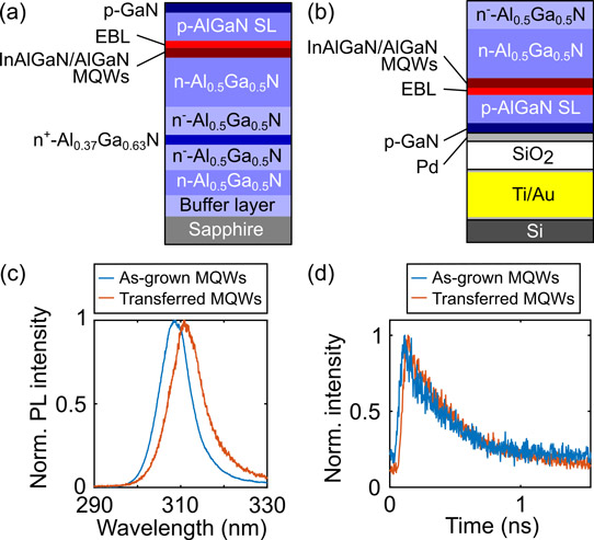
A multiple quantum well (MQW) structure was grown on a 130nm Al0.37Ga0.63N sacrificial layer to show that the electrochemical etch could be used without affecting device performance (Figure 2). The 2x10¹⁸/cm3 {Si] Al0.5Ga0.5N 4μm-thick underlayer was relaxed. The sacrificial layer aluminium content was chosen to be transparent for photoluminescence (PL) analysis but low enough to contrast with the surrounding layers.

Figure 2: (a) As-grown MQW sample structure, (b) transferred MQW-containing structure, (c) PL spectrum of as-grown MQW probed from Ga-polar side and transferred structure probed from etched N-polar side, and (d) time-resolved PL of structures.
The MQWs were indium aluminium gallium nitride with 21% Al content. The three wells were 2nm thick, separated by 5nm Al0.3Ga0.7 barriers. The magnesium-doped p-type layers were an Al0.75Ga0.25N electron-blocking layer, an AlGaN superlattice (SL), and a 20nm p-GaN cap.
The material was prepared for electrochemical etching by dry reactive-ion etching circular mesas. Palladium was deposited on the p-GaN cap. The mesas were partially covered with 1μm sputtered silicon dioxide (SiO2) to prevent parasitic etching during the electrochemical process. Finally, a titanium/gold bond pad was deposited on the palladium.
The electrochemical etch potential was 25V. The released structures were transferred to silicon carriers with titanium/gold bonding layer using a 300°C thermos-compression process.
The PL analysis showed a small red-shift after transfer. The researchers report “This shift of 2nm could be caused by small local variations in the Al-composition and thickness over the sample, residual strain in the epitaxy, and process-induced strain.”
Time-resolved measurements before and after transfer showed the same PL decay rate of 340ps. The team concludes: “This confirms that the electrochemical etching and transfer process do not influence the quality of the QWs and, hence, are an appropriate process for fabrication of devices based on free-standing membranes.”
https://doi.org/10.1063/1.5120397
The author Mike Cooke is a freelance technology journalist who has worked in the semiconductor and advanced technology sectors since 1997.


