


- News
21 November 2019
Boost to magnesium doping of gallium nitride on freestanding substrates
Japan’s National Institute for Materials Science (NIMS) has found that magnesium doping of gallium nitride (GaN:Mg) is far more effective in material grown homoepitaxially on freestanding substrates as opposed to GaN/sapphire templates [Liwen Sang et al, Appl. Phys. Lett., vol115, p172103, 2019].
The researchers point to the reduction of self-compensation as the basis for the enhanced doping performance. Self-compensation occurs where acceptor states are neutralized by the generation of parasitic deep-donor non-radiative recombination centers (NRCs). Also, the reduced numbers of threading dislocations in material grown on freestanding substrates is thought to reduce Mg diffusion effects that adversely affect doping performance.
Freestanding substrates can have threading dislocation densities as low as 104/cm2, some three orders of magnitude lower than for GaN/sapphire templates. Of course, freestanding substrates are significantly more expensive than the templates, but the development of potential application opportunities and substrate production technology should encourage economies of scale in future.
The enhanced GaN:Mg on freestanding substrates was found to have five to ten times the free hole density, implying higher conductivity. In addition, one would expect higher mobility if lower magnesium concentration can be used due to reduced impurity scattering.
Another potential use of p-GaN is as a current-blocking layer in vertical metal-oxide-semiconductor field-effect transistors (MOSFETs) and current-aperture vertical electron transistors (CAVETs). The creation of p-GaN:Mg during epitaxial growth is preferred over ion implantation. The latter process suffers from excessive out-diffusion of the dopants during thermal anneal processes.
Metal-organic chemical vapor deposition (MOCVD) was used to grown 1μm Mg-doped GaN on c-plane n+-GaN freestanding substrates with 4x10⁶/cm2 threading dislocation density. The growth temperature was 1000°C and bis(methylcyclopentadienyl) magnesium was the precursor for the doping. The Mg-doped layer was grown on an undoped 2μm GaN buffer with 5x10¹⁵/cm3 free electron density. The Mg doping was activated with 30-minute annealing at 725-820°C.
One effect of using GaN substrates was narrow peaks in x-ray diffraction (XRD) rocking curves (Figure 1): 68arcsec full-width at half maximum (FWHM) for the (002) plane and 95arcsec for (102). These values correspond to a threading dislocation density of 7x10⁶/cm2. The same growth process, but using GaN/sapphire templates, led to FWHM values of 280arcsec and 491arcsec for the (002) and (102) planes, respectively. The estimated threading dislocation density in this case was 6x10⁹/cm2, almost three orders of magnitude higher than for the GaN:Mg on freestanding substrate.
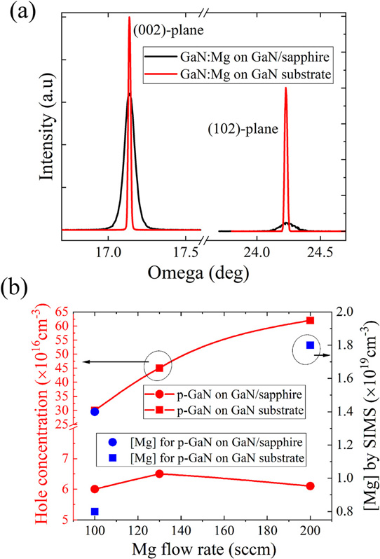
Figure 1: (a) XRD omega rocking curves of (002)- and (102)-plane reflection for homoepitaxial and heteroepitaxial GaN:Mg films. (b) Free hole concentration and [Mg] values for homoepitaxial and heteroepitaxial GaN:Mg films.
Hall measurements with lightly doped GaN on GaN/sapphire template with 1.4x10¹⁹/cm3 {Mg} concentration gave a 6x10¹⁶/cm2 free hole density. Homoepitaxy on freestanding GaN increased the free hole concentration five-fold to 3x10¹⁷/cm3 with a reduced {Mg} of 8x10¹⁸/cm3. The higher Mg incorporation on sapphire was attributed to a higher density of edge-type dislocations.
Heavier Mg-doping resulted in free hole concentrations of 6.0x10¹⁷/cm3 on freestanding substrate (1.8x10¹⁹ Mg concentration). This was ten times the 6.1x10¹⁶/cm3 on sapphire for the same Mg flow. The team comments: “The marked enhancement of the doping efficiency is attributed to the suppression of the Mg-related self-compensation centers or non-radiative recombination centers benefitting from the greatly reduced dislocation density.”
The researchers also found that the relation between photoluminescence (PL) spectral structure and p-type conductivity in GaN:Mg was different on freestanding GaN substrates, compared with heteroepitaxy on sapphire (Figure 2).
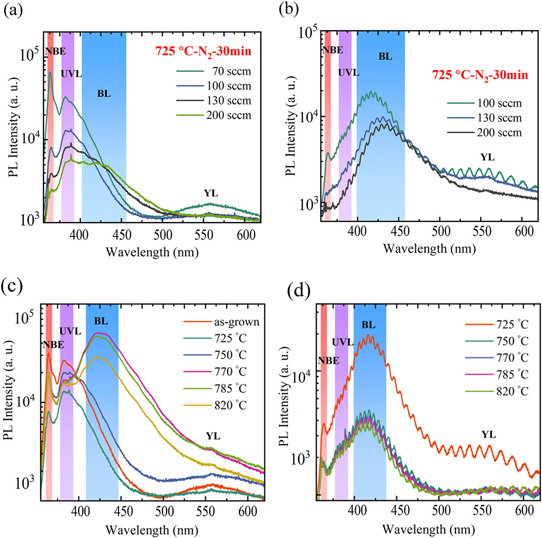
Figure 2: PL spectra of p-GaN films grown on (a) GaN substrates and (b) GaN/sapphire templates activated at 725°C in N2 with different Mg doping concentrations. (c) and (d) PL spectra of homoepitaxial and heteroepitaxial GaN:Mg films activated at varying temperatures, respectively.
With heteroepitaxial GaN:Mg a blue-band luminescence (BL, ~2.9eV) is associated with onset of p-conductivity. This luminescence is generally attributed to deep donor-acceptor pair (DAP) recombination.
By contrast the NIMS researchers found that ultraviolet luminescence (UVL, ~3.26eV) was the signal for homoepitaxial GaN:Mg on freestanding GaN to be p-type conducting. These emissions were attributed to free electron or shallow donor recombination with acceptor levels.
The PL spectra also include near-band-edge (NBE) emissions and yellow luminescence (YL). The YL emissions are attributed to electron transitions into deep acceptor levels associated with carbon atoms on nitrogen sites.
The homoepitaxial GaN:Mg had increased ultraviolet luminescence with increased activation anneal temperatures up to 750°C, but then BL emissions started appearing, indicating reduced effectiveness. The higher activation temperatures also resulted in increased surface roughness measured using atomic force microscopy: 0.81nm root mean square at 770°C, compared with 0.25nm at 725°C.
The NIMS team comments: “The rough morphology deteriorates the luminescence behaviors, which is related to the increased thermal emission of electrons from donor levels to the conduction band and their recapture by the non-radiative recombination centers on the rougher surface. The electrical current of Ohmic contacts is reduced when the activation temperature is higher than 750°C.”
X-ray photoelectron spectra (XPS) indicated that homoepitaxy also improved the uniformity of surface states, avoiding regions with excess Mg-Ga-O. Such excess Mg-Ga-O inhibits abrupt interfaces when growing aluminium oxide dielectric. Abrupt interfaces are desired for metal-oxide-semiconductor structures in vertical field-effect transistors with high mobility and stable positive threshold voltages.
Magnesium doping MOSFETs GaN MOCVD CAVETs GaN substrates
https://doi.org/10.1063/1.5124904
The author Mike Cooke is a freelance technology journalist who has worked in the semiconductor and advanced technology sectors since 1997.


