


- News
7 November 2019
Indium phosphide template for laser and silicon-on-insulator integration
Hewlett Packard Labs (HP) and University of California Santa Barbara (UCSB) in the USA have reported on their work on integrating 1.3μm-wavelength III-V laser diodes on a silicon (Si) platform [Yingtao Hu et al, Light: Science & Applications, vol8, p93, 2019]. The HP/UCSB method (Figure 1) combines the two usual approaches to integration of the III-V devices on silicon – direct wafer bonding and direct epitaxy on silicon – by transferring an indium phosphide (InP) layer to a silicon-on-insulator (SOI) substrate, forming a growth surface for subsequent metal-organic chemical vapor deposition (MOCVD).
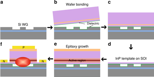
Figure 1: Schematic of III-V/Si integration.
Direct epitaxy suffers from performance and lifetime degradation due to defect generation from lattice and thermal expansion mismatching between III-V compound semiconductors and silicon. Threading dislocations typically reach densities of the order 108/cm2. The attractions of direct epitaxy over wafer bonding include the less expensive substrate cost and economies of scale from the use of large-diameter wafers.
The aim is the integration of electronics with a complete photonics platform on silicon, from light generation, transmission through waveguides and fibers, and detection. Apart from light generation, transmission and detection can be efficiently accomplished using Si-based systems. “Silicon photonics is becoming a mainstream data-transmission solution for next-generation data centers, high-performance computers, and many emerging applications,” the researchers comment.
Adding efficient III-V light generation should enable a wide range of new and old electronic, photonic and micro-electro-mechanical system (MEMS) applications, by supplying light sources, amplifiers, modulators and detectors on a single chip with close proximity and low coupling loss.
The researchers foresee the ability to integrate lasers, amplifiers, modulators and photodetectors onto the bonding plus epitaxy integration platform, using multiple selective regrowth steps. The team also suggests that the source InP growth substrate could be used multiple times to transfer template layers to a number of SOI platforms, reducing material costs.
The 4-inch SOI substrate with 350nm Si top layer and 1μm buried oxide was prepared with waveguides and out-gassing structures etched into the silicon layer (Figure 1). The 150nm-thick n-InP template layer was applied from a 2-inch wafer that included the growth substrate and 200nm InGaAs etch-stop layer.
The template was wafer bonded to the silicon with an intermediate 7nm atomic layer deposition (ALD) silicon dioxide dielectric layer on both sides of the bond. The researchers used a cleaved quarter patterned SOI wafer. The InP template wafer was also quartered. The bonding was strengthened by a 300°C annealing step. The InP growth substrate and InGaAs etch stop were then removed. Presumably, in future multiple-use contexts, the growth substrate would be removed by some non-destructive process such as laser lift-off or ion-implantation (e.g. Soitec’s smartcut process) rather than the destructive mechanical polishing/grinding and wet etching, as here.
The InP template layer was found to be strained due to thermal expansion mismatch between it and the underlying silicon. The strain was found to be ~1250-parts-per-million compressive in x-ray analysis.
MOCVD at 600°C on the n-InP template resulted in a ~2μm vertical p-i-n epitaxial structure for standard laser diode fabrication. The target wavelength for emission from the 102nm six-period indium gallium arsenide phosphide (InGaAsP) multiple quantum well (MQW) active region was 1.31μm. The MQW was grown on a 50nm separate-confinement heterostructure (SCH) layer on the 150nm n-InP template. Following on from the MQW were 150nm SCH, 1.5μm p-InP cladding, and 200nm p-InGaAs contact.
The bonded structure avoided the usual lattice and charge-polarity mismatches between silicon and III-V materials. This meant that thick buffer layer transitions from silicon to the III-V layer was not required. In addition, the laser structure was much closer to the underlying silicon waveguide systems, so that coupling into the silicon photonics waveguide platform should become much easier.
The researchers quantified the threading dislocation (TD) density at 9.4x10⁴/cm2, using electron-channeling contrast imaging on 100x14.5μmx14.5μm fields, resulting in the detection of 20 TDs. The team points out that this is only one order of magnitude higher than for material grown on native InP substrates, and two orders of magnitude lower than for “state-of-the-art conventional monolithic growth [on Si] with a thick buffer layer”. Further analysis found some small areas of higher TD density, which the researchers blame on bonding voids or included dirt particles.
Photoluminescence (PL) produced using a 780nm pump laser showed 2.53x the intensity of a sample grown on native InP. The researchers attribute the increase to strong reflection of the pump light from the underlying silicon and buried-oxide layers, creating a cavity effect. In both cases, the upper contact and cladding layers were removed.
The position of the PL peak for the sample on silicon was also shifted to a shorter wavelength of 1288.0nm, compared with 1305.5nm on native InP. The full-width at half maximum (FWHM) was also narrower in the bonded sample – 41.1meV, compared with 61.9meV on native InP.
The team explains: “The residual thermal strain in the MQWs of the bonded substrate sample likely caused the differences in the PL profile and wavelength. In addition, a slight difference in the growth temperature on the top surface of the bonded substrate and on the InP substrate due to the difference in their thermal conductivity could cause composition changes, thus leading to PL shifts. Nevertheless, the epitaxy quality on the bonded substrate is comparable with that on the InP substrate.”

Figure 2: (a) Room-temperature pulsed voltage and light output power against current (inset: microscope image). (b) Pulsed light output versus current up to 40°C (inset simulated mode profile at facets). (c) Device spectrum. (d) Continuous-wave light output power versus current up to 20°C (inset: scanning electron micrograph (SEM) of hybrid facet). (e) Room-temperature pulsed performance with silicon waveguide at laser facet (inset: microscope image of device and SEM of taper). (f) Pulsed light output versus current up to 35°C (inset: simulated mode profile at facets).
Fabry-Perot ridge-laser bars on silicon with a 1.9mm-long cavity (Figure 2) had a threshold current of 61.8mA (813A/cm2). The 4μm-wide p-channel was defined using proton implantation, followed by etching of an 8μm-wide mesa. The device surfaces also were passivated with 800nm of silicon dioxide.
At 120mA injection, the output power from a single facet was 4.2mW. The slope efficiency was 0.14W/A. These measurements were made at 20°C room temperature with 0.5μs current pulses at 0.25% duty cycle. Continuous-wave operation increased the threshold to around 80mA due to self-heating effects. The peak wavelength was at 1313nm.
The researchers report some processing problems such as a 10x higher zinc doping concentration in the p-InP cladding than intended. This caused light absorption that reduced efficiency. The p-contact metal process was also less than ideal and, along with a ‘problematic’ wet etch, increased electrical resistance.
https://doi.org/10.1038/s41377-019-0202-6
The author Mike Cooke is a freelance technology journalist who has worked in the semiconductor and advanced technology sectors since 1997.


