


- News
12 November 2019
University of Illinois reports thermal conductivity dependence on dislocation density of various GaN materials
Gallium nitride (GaN) materials are critical for energy conversion, communications and sensing but, despite material advantages, existing mainstream GaN photonic and electronic devices are limited by the thermal heat extraction, and one of the biggest challenges in GaN devices (including RF transistors and LEDs) is heat extraction.
A research team at the University of Illinois at Urbana-Champaign (UIUC) led by professor Can Bayram has now reported what is clamed to be the first systematic study of the thermal conductivity of gallium nitride materials with various dislocation densities, including hydride vapor phase epitaxy (HVPE)-grown GaN, high nitride pressure (HNP)-grown GaN, and metal-organic chemical vapor deposition (MOCVD)-grown GaN on sapphire (GaN/sapphire) and on silicon (111) (GaN/Si) – see K. Park and C. Bayram, ‘Impact of dislocations on the thermal conductivity of gallium nitride studied by time-domain thermoreflectance’, J. Appl. Phys. 126, 185103 (2019).
GaN thermal conductivities (κGaN) of HVPE GaN, HNP GaN and MOCVD-grown GaN/sapphire and GaN/Si are measured as 204.7(±4.6), 206.6(±6.8), 191.5(±10.5) and 164.4(±3.2)W/m.K, respectively, using time-domain thermoreflectance (TDTR). Dislocation densities (σD) of HVPE GaN, HNP GaN, GaN/sapphire, and GaN/Si are measured as 4.80(±0.42)x105, 3.81(±0.08)x106, 2.43(±0.20)x108 and 1.10(±0.10)x109cm-2, respectively, using cathodoluminescence and XRD. Impurity concentrations of Si, H, C and O are measured by secondary-ion mass spectroscopy (SIMS) to complement the analysis.
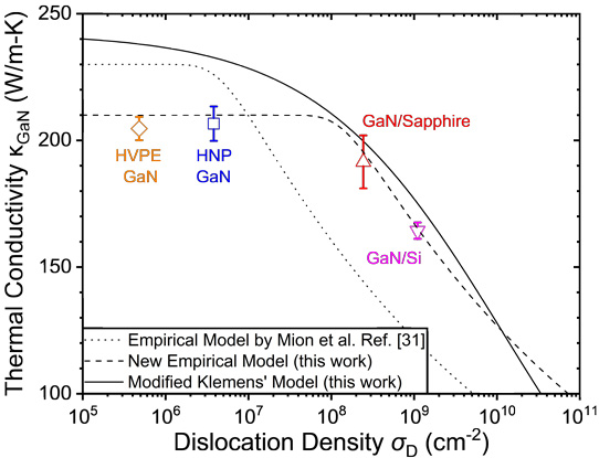
Graphic: Effect on thermal conductivity of dislocation density in various GaN materials. κGaN of HVPE GaN, HNP GaN, GaN/sapphire and GaN/Si as a function of σD (open symbols). Empirical model by Mion et al [Appl. Phys. Lett. 89, 092123 (2006)], κGaN = 230tanh0.12(5×10⁶/σD) (dotted line), new empirical model, κGaN = 210 tanh0.12(1.5×10⁸/σD) (dashed line, University of Illinois work), and modified Klemens’ model (solid line, University of Illinois work) are plotted together for comparison.
Using the experimental data, the team proposes a new empirical model to describe how thermal conductivity of GaN is affected by dislocation density, specifically κGaN = 210tanh0.12(1.5x10⁸/σD). They also propose a modification in Klemens’ model, where dislocation-induced scattering strength is increased, to explain the experimental rate of decrease in thermal conductivity with increasing dislocation density.
Their empirical expression provides a means to estimate the thermal conductivity of heteroepitaxially grown GaN samples indirectly by determining the dislocation density which is, in many cases, simpler than directly measuring the thermal conductivity.
The team reckons that the work provides key design guidelines for the thermal management of GaN-based devices, typically grown on foreign substrates with high dislocation densities.


