


- News
24 October 2019
High-carrier-density two-dimensional hole gas in strained gallium nitride
Cornell University in the USA reports a high-conductivity two-dimensional hole gas (2DHG) in gallium nitride (GaN) that could enable high-voltage circuits using more power-efficient complementary combinations of n- and p-channel transistors [Reet Chaudhuri et al, Science, vol365, p1454, 2019].
Since the work described in the Science paper, Chaudhuri and fellow researcher Samuel James Bader have realized what is described in a press release as “some of the most efficient p-type GaN transistors in a collaborative project with Intel”.
Combining the p-type transistors with more conventional and developed n-type devices could lead to a range of opportunities in high-power switching, 5G cellular technology and energy-efficient electronics, including phone and laptop chargers, using more complex circuitry.
Another co-senior author, Huili Grace Xing, comments: ““It’s very difficult to simultaneously achieve n-type and p-type in a wide-bandgap semiconductor. Right now, silicon carbide is the only other one that has both besides GaN. But the mobile electrons in silicon carbide are more sluggish than those in GaN. Using these complementary operations enabled by both n-type and p-type devices, much more energy-efficient architecture can be built.”
“Silicon is very good at switching off and on and controlling electrical energy flow, but when you take it to high voltages it doesn’t operate very well because silicon has a weak electric strength, whereas GaN can sustain much higher electric fields,” adds co-senior author Debdeep Jena. “If you’re doing very large amounts of energy conversion, then wide-bandgap semiconductors such as GaN and silicon carbide are the solutions.”
Cornell’s 2DHG depends on similar principles to the more usual 2D electron gas (2DEG) when aluminium gallium nitride (AlGaN) is grown on GaN. Such 2DEGs are the basis for high-frequency, high-power and/or high-voltage n-channel transistors being developed for wireless network power amplifiers, power switching, and other applications.
The 2DEG results from the broken inversion symmetry of the III-nitride lattice structure with the bonds between the atoms being strongly ionic – i.e. the charge density tends around the Ga and Al metal ions to be positive, and around the N atoms negative. There are both spontaneous and strain-dependent (‘piezoelectric’) charge polarizations. Within homogeneous regions, the net charge is zero, but at interfaces between different material compositions an interface charge develops that is due to the difference in charge polarization on each side. The charge in the case of AlGaN/GaN induces a 2DEG nearby, mostly in the GaN buffer.
The Cornell strategy for its 2DHG was to grow a thin strained-layer of GaN pseudomorphically on a thick relaxed AlN buffer. This reverses the situation for the conventional 2DEG where the AlGaN is a thin layer on a relaxed GaN buffer.
The contrast of charge polarization at the strained GaN on AlN was expected to create a negative interface charge of order 5x10¹³/cm2, inducing a compensating 2DHG nearby. The valence band offset between the materials should push the 2DHG to mainly reside in the strained GaN layer.
The experimental samples were produced using plasma-assisted molecular beam epitaxy (PAMBE) on sapphire. X-ray analysis suggested that the GaN layer was compressively strained 2.4%.
In addition to the main 13nm/400nm GaN/AlN sample A, the researchers also produced variations for comparison: sample B with magnesium-doped p-GaN replacing the top 10nm of the GaN layer, and sample C with a thick magnesium-doped GaN layer directly on the sapphire substrate. Sample B was designed “to lock the Fermi level to valence band edge separation, screening the 2DHG from variations of the surface potential”; sample C was intended as a control comparison with conventional acceptor doping.
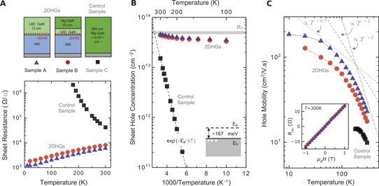
Figure 1: Magneto-transport measurements between 300K and 10K with applied field of 1 Tesla (1T): (A) sheet resistance with schematics of samples; (B) sheet hole concentration, with inset scheme of activation/acceptor level energy (Ea) above valence band edge (EV); and (C) hole mobility, with inset Hall coefficient (Rxy) versus magnetic field (µ0H) at room temperature.
The temperature dependence of the resistivity of the control sample C, with higher values at low temperature, suggested an activation energy of ~170meV for the acceptor doping (Figure 1). The increased resistance was almost entirely related to the reduction in thermally excited holes, the researchers explain.
The team adds: “We observed a dramatically different behavior for the undoped heterostructure sample A and the Mg-doped heterostructure B. They showed metallic behavior, with the resistivity decreasing with decreasing temperature, which is a signature of a degenerate 2D hole gas.”
At a typical room temperature of 300K, the resistivity of sample A was 6.0kΩ/square, while B’s value came in at 8.0kΩ/square. The corresponding low-temperature values were 1kΩ/square (10K) and 2kΩ/square (20K). The hole densities in the 2DHG were considered to be relatively temperature independent. The reductions in resistivity thus suggest increases in mobility at low temperature.
The areal hole concentration of the 10nm p-GaN layer in sample B was around 5x10¹²/cm2, an order of magnitude lower than the expected 2DHG density. Hall measurements gave mobility values of 25cm2/V-s and 20cm2/V-s at room temperature for samples A and B, respectively. At very low temperature, the mobility increased to 190cm2/V-s for sample A at 10K, and 120cm2/V-s for sample B at 20K.
The researchers comment: “The variation of the measured 2D hole gas mobility with temperature is expected to be strongly influenced by acoustic phonon scattering, in addition to the polar optical phonon scattering that dominates in most polar compound semiconductors.”
The undoped sample A mobility was not saturated at 10K and the researchers suggest that values of 200cm2/V-s could be reached. This would allow the use of magneto-transport studies for detailed probing of the GaN valence band.
Two-dimensional holes gases were observed in a number of heterostructures similar to the main samples A and B presented in the paper. The team reports: “The 2DHG densities of ~5x10¹³/cm2 measured in this work are near the expected polarization difference and much higher than previously reported 2DHG densities in nitride semiconductors [Figure 2].”
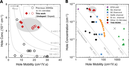
Figure 2: Comparisons with other reported 2DHGs: (A) in III-nitrides; (B) other semiconductor material systems – strontium titanium oxide/lanthanum aluminium oxide (STO/LAO), germanium (Ge), silicon inversion (Si inv.), gallium antimonide (GaSb), semiconducting (SC) diamond.
The 2DHG concentration also beats the values in other semiconductor systems. At the same time, compared with narrower-bandgap semiconductors, the III-nitride ‘light’ and ‘heavy’ holes tend to have higher effective masses, reducing mobility. “However, a large bandgap means that the high 2D hole gas densities can be modulated effectively with a gate through field effect because the semiconductor intrinsically is capable of sustaining much larger electric fields,” the team writes.
The polarization-based doping effect has another advantage – uniformity down to the atomic scale in contrast to the fluctuations of dopant concentration in the more usual magnesium-doped p-GaN.
2DHG GaN AlGaN SiC 5G cellular PAMBE
https://doi.org/10.1126/science.aau8623
The author Mike Cooke is a freelance technology journalist who has worked in the semiconductor and advanced technology sectors since 1997.


