


- News
17 October 2019
Silicon carbide 600V transistors comparable to silicon performance
North Carolina State University in the USA has implemented its 4H-polytype silicon carbide (SiC) inversion-channel power metal-oxide-semiconductor field-effect transistor (MOSFET) technology on a 6-inch foundry process, achieving 600V high-voltage rating and 15V gate drive [Aditi Agarwal, Kijeong Han, and B. Jayant Baliga, IEEE Electron Device Letters, published online 18 September 2019]. The 15V gate-drive value makes the technology compatible with insulated-gate bipolar transistor (IGBT) circuitry.
The team reports: “The high-frequency figures-of-merit (HF-FOMs) of the SiC MOSFETs with 27nm gate oxide were found to surpass that of commercially available 600V P7 Si CoolMOS™ products for the first time.” Up to now, SiC-based devices have found it difficult to beat the performance of 600V-rated silicon products, inhibiting adoption of the technology.
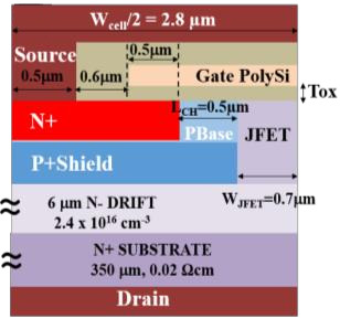
Figure 1: Schematic cross section for fabricated linear cell MOSFET devices.
The inversion-channel devices (Figure 1) were manufactured at a commercial foundry facility run by X-Fab on 6-inch SiC wafers. The gate oxide thickness (Tox) was 27nm; the channel was 0.5μm long. The fabrication of the drift region used NCSU’s trade-marked PRESiCE process. The gate oxide was created through thermal oxidation at 1175°C for 150 minutes. A comparison device with 55nm oxide used a 300-minute oxidation process. The resulting device active area was 0.045cm2.
Simulations of the structure suggested that the peak field in the off-state would be in the middle of the JFET region. The peak field in the gate oxide with 600V drain bias was 3.2MV/cm (2.8MV/cm for 55nm thick oxide). A value of 4MV/cm is considered to be the threshold where block-state operation becomes unreliable.
In the on-state, with 15V on the gate, the simulated peak oxide field was 5.6MV/cm (3.6MV/cm for 55nm). The researchers believe this large on-field is acceptable, “because an oxide electric field of 6MV/cm at 175°C will result in stable on-state operation for 1000 years.”
For the fabricated devices, the threshold voltages for 1mA current with 0.1V drain bias were 1.9V and 3.56V for the 27nm and 55nm oxides, respectively. The corresponding transconductances at 10A/20V drain current/voltage were 8.5S and 5.5S. The higher transconductance for the 27nm-oxide transistor should enable faster switching.
Comparing the on-resistance at gate potentials of 15V and 20V for the 27nm- and 55nm-oxide MOSFETs, respectively, showed a 1.7x smaller value in the 27nm case. The effective channel-inversion mobilities in the two cases were similar, of the order 15cm2/V-s, so the lower on-resistance was the result of the normal field from the gate creating a higher carrier density in the channel in the 27nm case.
The specific on-resistance with the gate potential in the 10-15V range for the 27nm is similar to that for 55nm-MOSFET in the 20-25V range. The team comments: “Reducing the gate drive voltage to the 10–15V range with the 27nm gate oxide thickness allows the use of widely available 15V gate drivers previously developed for Si IGBTs.”
The blocking voltage (BV) for 100μA leakage current (Ileakage) was 846V for 27nm oxide, greater than that the 703V value for 55nm. “We believe that this is due to a combination of increased field-plate effect, or differences in drift region doping and/or thickness for the two wafers,” the researchers write.
Statistically analyzing the performance variation across the wafers, the leakage current was in the nA range at 600V drain bias (Figure 2). The specific on-resistance of the 27nm-oxide MOSFETs was just over half that of the 55nm version. The breakdown voltage for all the 27nm devices was well above 600V.
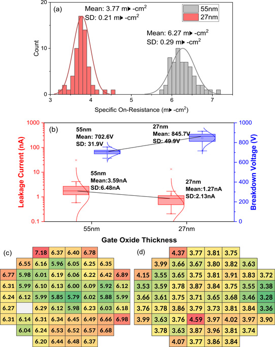
Figure 2: (a) Statistical distributions of Ron,sp for 55nm and 27nm gate oxide MOSFETs at 20V and 15V gate potential, respectively; (b) box plots of leakage current (red) at 600V and BV (blue) at 100μA; (c) wafer-map of Ron,sp for 55nm device at 20V gate voltage and 10A drain current, and (d) for 27nm device at 15V gate and the same drain current.
The researchers report: “The Ron,sp mean and best value of 3.77 and 3.28mΩ-cm2 for the 27nm devices are smaller than that reported in previous papers for inversion-mode devices with linear cell topology.” They add: “The measured mean and standard deviation numbers for Ron,sp, BV and Ileakage demonstrate that the PRESiCE™ non-self-aligned foundry process is robust even for 27nm gate oxide MOSFETs.”
The thinner oxide also benefits a number of FOMs with respect to the various parasitic capacitances and related charge storage, One HF-FOM, the product of on-resistance and reverse-transfer capacitance (RonxCrss), was 1.7x lower in the 27nm-oxide MOSFET, compared with the 55nm version. Another HF-FOM, the product of Ron and the gate-drain charge (Qgd), was 1.6x lower. The ratio of input capacitance to reverse-transfer capacitance (Ciss/Crss) was improved by 1.5x: 185 for 27nm, and 120 for 55nm gate oxide.
The 934mΩ-nC RonxQgd for the 27nm gate oxide device compares favorably with the 1160mΩ-nC value for the commercial Infineon’s CooLMOS silicon product (IPW60R180P7). Rohm’s R6020JNZ4 SiC MOSFET only manages 3060mΩ-nC. On the other hand, the 834mΩ-pF RonxCrss FOM average for the 27nm-oxide device is somewhat higher than the 725mΩ-pF and 720mΩ-pF values for the commercial Si and SiC products, respectively. The best RonxCrss for the 27nm-oxide MOSFETs was in fact lower at 646mΩ-pF, so process optimization holds out the hope for consistent improvement over the commercial CooLMOS device.
The team comments: “The average and best FOM [RonxQgd] for the 27nm gate oxide device are 1.24× and 1.43× better than the Si P7 CooLMOS™ product, and its Ron,sp is 2.5× smaller. This demonstrates for the first time that 600V SiC power MOSFETs can be manufactured with superior performance compared to Si CooLMOS™ products, opening up new market opportunities for SiC technology.”
https://doi.org/10.1109/LED.2019.2942259
The author Mike Cooke is a freelance technology journalist who has worked in the semiconductor and advanced technology sectors since 1997.


