


- News
9 October 2019
High-frequency indium aluminium nitride barrier transistors on silicon
University of Delaware in the USA claims a record for radio frequency (RF) performance of indium aluminium nitride (InAlN)-barrier gallium nitride (GaN) high-electron-mobility transistors (HEMTs) on silicon [Peng Cui et al, Appl. Phys. Express, vol12, p104001, 2019]. The device also demonstrates records for direct current (DC) characteristics such as low gate leakage, high on/off current ratio, and subthreshold swing, according to the researchers.
Usually for high performance, GaN HEMTs are produced on very expensive silicon carbide (SiC) substrates. Growth on low-cost, large-diameter silicon should open up more economic opportunities for high-power and high-frequency GaN-based devices.
Metal-organic chemical vapor deposition (MOCVD) on (111) resulted in an epitaxial structure with a 2μm undoped GaN buffer, a 4nm In0.12Ga0.88N back-barrier, a 15nm GaN channel, a 1nm AlN interlayer, an 8nm lattice-matched In0.17Al0.83N barrier, and a 2nm GaN cap. Hall measurements gave sheet electron concentration and electron mobility values in the two-dimensional electron gas (2DEG) channel of 2.28x10¹³/cm2 and 1205cm2/V-s, respectively.
Device fabrication included plasma reactive-ion etch of isolation mesas, and alloying of titanium/aluminium/nickel/gold ohmic source-drain contacts at 850°C. The source-drain distance was 2μm. The researchers used an oxygen plasma treatment to oxidize the surface between the source and drain with the aim of reducing gate leakage current (Ig) and improve RF performance. The 80nm-long nickel/gold gate was centered in the source-drain gap.
The oxygen plasma treatment increased the on/off current ratio (Ion/Ioff) by a factor of around two to reach 1.58x10⁶. Another benefit was a reduction in subthreshold swing (SS) from 76mV/decade to 65mV/decade.
The team comments: “To the best of our knowledge, these DC measurement results all show record values among those reported InAlN/GaN HEMTs on silicon to-date (Ig of 7x10⁻⁶A/mm, Ioff of 7x10⁻⁶A/mm, Ion/Ioff ratio of 1.78x10⁵, and SS of 82mV/decade are the best values that have been reported in InAlN/GaN HEMTs).”
The researchers admit that better values have been obtained for Ig and Ioff with 20nm aluminium gallium nitride (AlGaN) barrier HEMTs on silicon – of order 10-12A/mm for both. The resulting Ion/Ioff was 2.5x10¹¹.
However, one benefit of the thinner InAlN-based barrier was better electrostatic control of current flow in the channel, reducing short-channel effects (SCEs). The InGaN back barrier reduces losses from current leaking into the buffer layer and improves confinement of charge carriers to the GaN-channel region.
The peak transconductance of the InAlN-HEMT was 391mS/mm with 10V drain bias, beating a 75nm-gate 11.4nm-barrrier AlGaN-HEMT’s 374mS/mm that has been reported. An 80nm-gate AlN-HEMT on silicon has been presented with 580mS/mm peak transconductance, enabled by a very thin 6nm barrier.
The 1.26A/mm maximum drain current of the team’s InAlN-HEMT has also been bettered by a similar device on silicon with a very small 300nm source-drain gap (2.66A/mm). The wider 2μm gap of the team’s HEMT naturally increased the on-resistance. One would expect, although the paper does not report on this, that the wider gap would lead to a higher breakdown voltage performance.
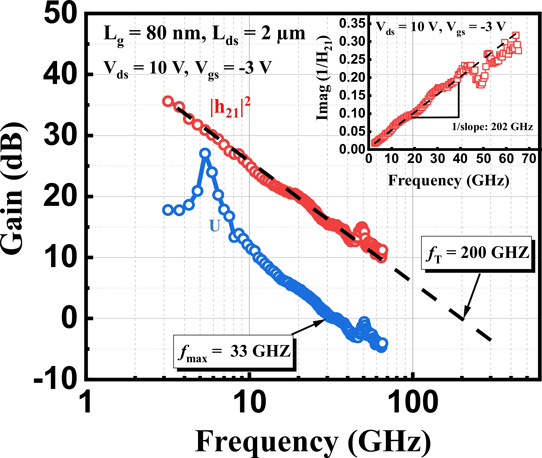
Figure 1: RF performance of 80nm-gate-length InAlN/GaN HEMTs with 200/33GHz fT/fmax. Inset: Gummel’s method showing 202GHz fT estimate.
RF measurements were made in the 1-65GHz range (Figure 1). With parasitic elements accounted for (“de-embedded”), the current gain cut-off (fT) was extracted as 200GHz, using a -20dB/decade extrapolation. The drain bias was 10V and the gate potential was set at -3V. The maximum oscillation/power gain (fmax) was 33GHz, suffering due to losses from the high resistance of the rectangular gate.
The cut-off-gate-length product (fTxLg) was 16GHz-μm. The researchers compare this with best result obtained on SiC – 17.8GHz-μm from 162GHz fT and 110nm Lg. The team comments: “To the best of our knowledge, the fTxLg in our study achieves the highest value among all reported GaN HEMTs on silicon, and set a new record among GaN HEMTs on SiC/Si with Lg ⩽ 100nm.”
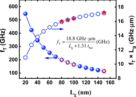
Figure 2: Predicted fT (left) and fTxLg (right) as a function of Lg - stars represent experimental results.
Using an empirical model that relates fT to Lg, barrier thickness, the effective electron velocity and one fitting parameter, the researchers project that an fT of 546GHz could be achieved with 20nm Lg, giving a fTxLg value of 10.9GHz-μm (Figure 2).
https://iopscience.iop.org/article/10.7567/1882-0786/ab3e29
The author Mike Cooke is a freelance technology journalist who has worked in the semiconductor and advanced technology sectors since 1997.


