


- News
18 September 2019
FBH reports 1.8kV-breakdown gallium oxide MOSFET with record power figure of merit
The Ferdinand-Braun-Institut, Leibniz-Institut für Höchstfrequenztechnik (FBH) of Berlin, Germany has developed gallium oxide (ß-Ga2O3) metal-oxide-semiconductor field-effect transistors (MOSFETs) that provide a high breakdown voltage combined with high current conductivity (K. Tetzner et al., ‘Lateral 1.8 kV β-Ga2O3 MOSFET With 155 MW/cm2 Power Figure of Merit’, IEEE Electron Device Letters, vol. 40, no.9 (September issue), p1503-1506).
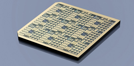
Picture: Gallium oxide chip with transistor structures and structures for measurement purposes, manufactured at FBH using projection lithography (photo courtesy of FBH/schurian.com).
Powerful electronic components are indispensable for future communications, for both the digital transformation of society and for artificial intelligence applications, notes FBH. On a footprint as small as possible, they should offer low energy consumption and achieve ever higher power densities, thus working more efficiently. This is where conventional devices reach their limits. Researchers all over the world are therefore investigating new materials and components that can meet these requirements.
With a breakdown voltage of 1.8kV and a record power figure of merit of 155MW/cm2, the new ß-Ga2O3-MOSFETs achieve what are said to be unique performance figures close to the theoretical material limit of gallium oxide. At the same time, the breakdown field strengths achieved are significantly higher than those of established wide-bandgap semiconductors such as silicon carbide (SiC) or gallium nitride (GaN).
To achieve these improvements, the FBH team optimized the layer structure and gate topology. The basis was provided by substrates from the Leibniz-Institut für Kristallzüchtung with an optimized epitaxial layer structure. As a result, the defect density could be reduced and electrical properties improved. This leads to lower on-state resistances. Since the gate is the central ‘switching point’ of a field-effect transistor (controlled by the gate-source voltage), its topology has been further optimized, allowing a reduction in the high field strengths at the gate edge. This in turn leads to higher breakdown voltages.
Ga2O3 Gallium oxide transistors


