


- News
25 September 2019
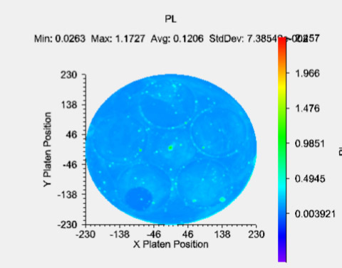
kSA Emissometer for MOCVD wafer carrier characterization gains UV PL capabilities
k-Space Associates Inc of Dexter, MI, USA - which supplies in-situ, ex-situ and in-line metrology tools for the thin-film, semiconductor, photovoltaic (PV), solar, automotive, glass and building materials industries – says that the kSA Emissometer ex-situ metrology tool for metal-organic chamical vapor deposition (MOCVD) carrier characterization now has ultraviolet (UV) photoluminescence (PL) capabilities for even better carrier evaluation.
The new UV PL feature allows wafer carrier manufacturers, reactor manufacturers and epi houses to further evaluate their wafer carriers before use and throughout their lifecycle. The system uses a 365nm-wavelength LED focused on the wafer carrier and a filtered photodetector focused on the excitation point. The filter cuts off light for wavelengths shorter than 409nm. This results in the ability to evaluate contamination on the wafer carrier.
The kSA Emissometer is used to determine the quality of the carrier bake after the deposition run, quantitative determination of real surface emissivity for temperature set-point adjustments, and microcrack detection. It also provides statistical analysis of each individual pocket and web for carrier quality evaluation.
“This tool gives carrier manufacturers, reactor manufacturers and epi houses a competitive edge because it allows them to quantify their carrier quality, ultimately leading to increased device uniformity and increased yield,” says CEO Darryl Barlett.


