| Home | About Us | Contribute | Bookstore | Advertising | Subscribe for Free NOW! |
| News Archive | Features | Events | Recruitment | Directory |
| FREE subscription |
| Subscribe for free to receive each issue of Semiconductor Today magazine and weekly news brief. |
News
13 December 2006
MIT demonstrates InGaAs transistors that could succeed silicon
At this week’s IEEE International Electron Devices Meeting (IEDM) in San Francisco, CA, USA, the Massachusetts Institute of Technology (MIT) presented results on InGaAs-based high-electron mobility transistors (HEMTs) with thin InAlAs barrier layers that could succeed silicon in logic chips.
The increase in performance of CMOS-based ICs with shrinking of the constituent MOSFET transistors is expected to reach a limit for silicon within the next 10-15 years. “Unless we do something very radical pretty soon, the microelectronics revolution that has enriched our lives in so many different ways might come to a screeching halt,” says professor Jesus del Alamo, a member of MIT's Microsystems Technology Laboratories.
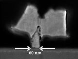
InGaAs has much higher electron mobility than silicon, but InGaAs HEMTs have previously been limited to transistor gate lengths of about 100nm. But using the capabilities of MIT’s Microsystems Technology Laboratories, Scanning-Electron-Beam Lithography Facility and the Nanostructures Laboratory, del Alamo’s group fabricated In0.7Ga0.3As quantum-well HEMT transistors on InP substrates using a thinner InAlAs barrier layer than before, allowing devices with a length of just 60nm size (similar to the most advanced 65nm silicon technology available). The devices can carry 2.5 times more current than state-of-the-art silicon devices and provide high performance at supply voltages as low as 0.5V. Del Alamo says that one reason for the performance of the transistors is the high quality of the epitaxial material, grown by epiwafer foundry MBE Technology of Singapore.
 The results were described as ‘a very important research milestone’ by Robert Chau, senior fellow and director of transistor research and nanotechnology at Intel, one of the sponsors of the research (along with Microelectronics Advanced Research Corp).
However, Del Alamo notes that InGaAs transistor technology is still in its infancy. Challenges include manufacturing transistors in large quantities, because InGaAs is more prone to breakage than silicon. But del Alamo expects prototype InGaAs microdevices at the required dimensions to be developed over the next two years and the technology to take off in a decade or so. "With more work, this semiconductor technology could greatly surpass silicon," he adds.
Visit:
http://web.mit.edu
![]() ©2006 Juno Publishing and Media Solutions Ltd. All rights reserved. Semiconductor Today and the editorial material contained within it and related media is the copyright of Juno Publishing and Media Solutions Ltd. Reproduction in whole or part without permission from Juno Publishing and Media Solutions Ltd is forbidden. In most cases, permission will be granted, if the author, magazine and publisher are acknowledged.
©2006 Juno Publishing and Media Solutions Ltd. All rights reserved. Semiconductor Today and the editorial material contained within it and related media is the copyright of Juno Publishing and Media Solutions Ltd. Reproduction in whole or part without permission from Juno Publishing and Media Solutions Ltd is forbidden. In most cases, permission will be granted, if the author, magazine and publisher are acknowledged.
Disclaimer: Material published within Semiconductor Today and related media does not necessarily reflect the views of the publisher or staff. Juno Publishing and Media Solutions Ltd and its staff accept no responsibility for opinions expressed, editorial errors and damage/injury to property or persons as a result of material published.
Semiconductor Today, Juno Publishing and Media Solutions Ltd, Suite no. 133, 20 Winchcombe Street, Cheltenham, GL52 2LY, UK
Web site by No Name No Slogan ![]()