
| Home | About Us | Contribute | Bookstore | Advertising | Subscribe for Free NOW! |
| News Archive | Features | Events | Recruitment | Directory |
New MEMS White Paper
Download the latest Logitech white paper and learn more about MEMS processing technology and techniques

| FREE subscription |
| Subscribe for free to receive each issue of Semiconductor Today magazine and weekly news brief. |
News
24 August 2007
Intel claims “first high-performance compound devices on silicon”
In a posting on the Research@Intel blog on Intel’s web-site, Mike Mayberry, director of Components Research at Intel’s Technology & Manufacturing Group, says that Intel has several active programs looking at compound semiconductors as a possible production option for mid next decade.
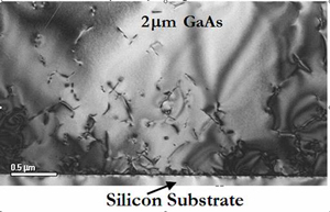 Picture: TEM of GaAs grown on silicon. The dark wavy lines are
dislocation defects that short out the device when you try to operate it.
“Gallium arsenide (GaAs) has about 8x higher mobility compared to silicon, and indium antimonide (InSb) has 50x higher,” points out Mayberry. “We’ve previously shown that you could achieve more than 10x improvement in power for an InSb device operating at 0.5V compared to the equivalent silicon device [reported at December 2005’s IEEE International Electron Devices Meeting],” he says. “We have to figure out how to make these in high volumes, which would be impossible if we were limited to small GaAs wafers as starting material [150mm, compared to 300mm-diameter silicon substrates].”
Mayberry says that Intel has broken down the overall problem into five challenges:
- Build compound semiconductor devices on silicon substrates. This would allow Intel to reuse the highly refined silicon infrastructure (including 300mm wafers) and give the option of integrating a few specialized devices with a ‘sea’ of silicon devices.
- Find a suitable high-k gate dielectric (due to the different surface, the high-k solutions used for silicon won’t work as-is).
- Build a compound PMOS device with high performance (comparable to existing compound NMOS devices to form power-efficient CMOS logic - although some circuits can get by with just one type).
- Build enhancement-mode devices (since most existing work is based on depletion mode, where a voltage is applied to shut them off, whereas power efficiency demands normally-off devices).
- Make the devices small enough to compete with leading-edge silicon transistor densities (if just a few specialized devices are integrated, then this is not needed, but that wouldn’t reap the full benefit of the technology).
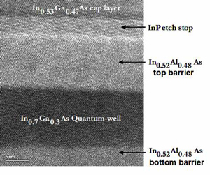
Picture: TEM of the quantum well (where electrical switching occurs),
showing the individual atomic layers.
Mayberry says that Intel is working on these challenges both in its internal labs as well as with external groups such as universities.
Regarding the first challenge, to grow working devices Intel first grows a buffer layer to absorb most of the lattice mismatch between the compound semiconductor and the silicon (which produces the defects that degrade device performance). Then, it grows a series of thinner layers with metamorphically graded alloy compositions with lattice spacings that, step by step, approach the desired value (the final layer is just a few tens of nanometers thick, so Intel currently uses molecular beam epitaxy to deposit each atomic layer individually).
Consequently, earlier this month Intel reported the fabrication of what Mayberry claims are the first high-performance compound devices on silicon (IEEE Electron Device Letters, Vol. 28, No. 8, August 2007, pp.685). Using either of two material types (InSb and InGaAs), in each case the performance is as good as their counterparts on GaAs wafers. Plots of the maximum frequency of depletion-mode devices against power dissipation for two InGaAs devices – one on indium phosphide and one on silicon - show that the two curves overlap each other, as well as showing significantly better performance (both higher cut-off frequency and lower DC power dissipation) than equivalently sized silicon devices.
In addition, at December’s IEDM 2007 conference, Intel intends to report newer results for much thinner buffer layers, as well as data on enhancement-mode devices.
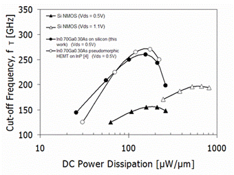
Picture: Maximum frequency of depletion-mode devices vs power dissipation for two InGaAs devices (one on indium phosphide and one on
silicon), showing that the two curves overlap each other, as well as showing
significantly better performance (both higher cut-off frequency and lower DC
power dissipation) than equivalently sized silicon devices.
Visit: Intel blog
![]() ©2007 Juno Publishing and Media Solutions Ltd. All rights reserved. Semiconductor Today and the editorial material contained within it and related media is the copyright of Juno Publishing and Media Solutions Ltd. Reproduction in whole or part without permission from Juno Publishing and Media Solutions Ltd is forbidden. In most cases, permission will be granted, if the author, magazine and publisher are acknowledged.
©2007 Juno Publishing and Media Solutions Ltd. All rights reserved. Semiconductor Today and the editorial material contained within it and related media is the copyright of Juno Publishing and Media Solutions Ltd. Reproduction in whole or part without permission from Juno Publishing and Media Solutions Ltd is forbidden. In most cases, permission will be granted, if the author, magazine and publisher are acknowledged.
Disclaimer: Material published within Semiconductor Today and related media does not necessarily reflect the views of the publisher or staff. Juno Publishing and Media Solutions Ltd and its staff accept no responsibility for opinions expressed, editorial errors and damage/injury to property or persons as a result of material published.
Semiconductor Today, Juno Publishing and Media Solutions Ltd, Suite no. 133, 20 Winchcombe Street, Cheltenham, GL52 2LY, UK
Web site by No Name No Slogan ![]()