| Home | About Us | Contribute | Bookstore | Advertising | Subscribe for Free NOW! |
| News Archive | Features | Events | Recruitment | Directory |
| FREE subscription |
| Subscribe for free to receive each issue of Semiconductor Today magazine and weekly news brief. |
News
4 January 2007
First p-type ZnO nanowires could lead to cheaper LEDs
Researchers at University of California, San Diego, in collaboration with Peking University's Electron Microscopy Laboratory, have reported the synthesis of the first high-quality p-type zinc oxide nanowires ('Rational Synthesis of P-type Zinc Oxide Nanowire Arrays Using Simple Chemical Vapor Deposition', Xiang et al, Nano Letters 2006 (Letter); doi: 10.1021/nl062410c). This could pave the way for a new, inexpensive type of LED that could compete with gallium nitride light-emitting diodes, the journal paper's authors claim.
For years, researchers have been able to make electron-rich, negatively charged n-type semiconducting ZnO nanowire crystals, but have not been able to make the hole-rich, positively charged p-type semiconducting ZnO nanowires that are also needed to form pn junctions in many electronic and optoelectronic devices, including LEDs. "ZnO is a wide-bandgap semiconductor, and generating p-type doping impurities that provide free holes is very difficult particularly in nanowires," says Deli Wang, senior author of the paper and electrical and computer engineering professor in UCSD¹s Jacobs School of Engineering.
Previously, p-type conduction in ZnO thin films has been demonstrated and ZnO thin-film LEDs have been fabricated. But using ZnO nanowires rather than thin films could be less expensive and lead to more efficient LEDs, reckons Wang. "ZnO nanostructures are incredibly well studied because they are so easy to make," he adds.
To make the p-type ZnO nanowires, the researchers doped ZnO crystals with phosphorus using a simple CVD technique (less expensive than the MOCVD technioque used to synthesize GaN-based LEDs). Adding phosphorus atoms to the ZnO crystal structure leads to p-type semiconducting materials through the formation of a defect complex that increases the number of holes relative to the number of free electrons. The starting materials and manufacturing costs for ZnO LEDs are far less expensive than those for GaN LEDs. In the future, Wang expects to cut costs even further by making p-type and n-type ZnO nanowires from solution.
Wang has filed a provisional patent for p-type ZnO nanowires. His lab is currently working on a variety of nanoscale applications. "Now that we have p-type ZnO nanowires, the opportunities for LEDs and beyond are endless," he says. "ZnO is a very good light emitter. Electrically driven ZnO single-nanowire lasers could serve as high-efficiency nanoscale light sources for optical data storage, imaging, and biological and chemical sensing," adds Wang.
Having both n- and p-type ZnO nanowires complementary nanowires could also be useful in a variety of applications including transistors, spintronics, UV detectors, nanogenerators, and microscopy. Transistors that rely on the semiconducting properties of ZnO are now on the horizon: "p-type doping in nanowires would make complementary ZnO nanowire transistors possible," says Wang. In spintronics applications, p-type ZnO nanowires could be used to make dilute magnetic semiconductors by doping ZnO with magnetic atoms, such as manganese and cobalt, he adds.
The research was funded by the US Office of Naval Research (ONR-nanoelectronics), the US National Science Foundation, and Sharp Labs of America.
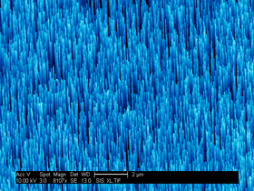
SEM image of p-type ZnO nanowires created by Deli Wang at UCSD. N.B The blue
color has been added. (Photo: Deli Wang/UCSD)
![]() ©2007 Juno Publishing and Media Solutions Ltd. All rights reserved. Semiconductor Today and the editorial material contained within it and related media is the copyright of Juno Publishing and Media Solutions Ltd. Reproduction in whole or part without permission from Juno Publishing and Media Solutions Ltd is forbidden. In most cases, permission will be granted, if the author, magazine and publisher are acknowledged.
©2007 Juno Publishing and Media Solutions Ltd. All rights reserved. Semiconductor Today and the editorial material contained within it and related media is the copyright of Juno Publishing and Media Solutions Ltd. Reproduction in whole or part without permission from Juno Publishing and Media Solutions Ltd is forbidden. In most cases, permission will be granted, if the author, magazine and publisher are acknowledged.
Disclaimer: Material published within Semiconductor Today and related media does not necessarily reflect the views of the publisher or staff. Juno Publishing and Media Solutions Ltd and its staff accept no responsibility for opinions expressed, editorial errors and damage/injury to property or persons as a result of material published.
Semiconductor Today, Juno Publishing and Media Solutions Ltd, Suite no. 133, 20 Winchcombe Street, Cheltenham, GL52 2LY, UK
Web site by No Name No Slogan ![]()