| Home | About Us | Contribute | Bookstore | Advertising | Subscribe for Free NOW! |
| News Archive | Features | Events | Recruitment | Directory |
New MEMS White Paper
Download the latest Logitech white paper and learn more about MEMS processing technology and techniques

| FREE subscription |
| Subscribe for free to receive each issue of Semiconductor Today magazine and weekly news brief. |
News
9 July 2007
Anadigics breaks ground for 6” GaAs fab in China
As part of a city-wide celebration in Kunshan, Jiangsu province, China, RFIC maker Anadigics Inc of Warren, NJ, USA has broken ground for construction of its new six-inch gallium arsenide wafer fabrication facility in the Kunshan New and Hi-Tech Industrial Development Zone (KSND), which was first announced in April.
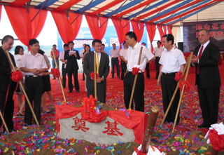
The ceremony took place with Kunshan party secretary Guohua Zhang, mayor Aiguo Guan and vice mayor Feng-Quan Zhu as well as several government officials along with Anadigics’ president and CEO Dr Bami Bastani, executive VP and chief technology officer Dr Charles Huang, and VP of worldwide human resources John Warren.
Driven by wireless and wireline broadband markets, in order to support Anadigics’ anticipated growth beyond its primary wafer fabrication in Warren, NJ, the firm and KSND plan to complete construction of the new fab in first-half 2008, and to make it operational in the latter part of the year.
“The addition of the commercial six-inch GaAs wafer fab to the development zone not only shows our ever-growing interest in the semiconductor industry but marks a historical first for the city of Kunshan and the country of China,” said Feng-Quan Zhu.
“Our new fab in China is a very significant development for both Anadigics and the city of Kunshan,” added Bastani. “Whereas the expansion will enable us to meet our future growth needs, it also demonstrates our commitment to the communications market in China as well as the larger Asia-Pacific Region.”
Anadigics said in April that it expects to invest $10-15m in capital expenditure over a two-year period. The total investment over the facility’s life-time (which could extend up to 50 years, the firm says) is estimated to be $ 49.88 m.
KSND consists of three sections within the city, involving many new and hi-tech industries including auto electronics, solar energy, robotics, and new materials. Located in Section B of the development zone, Anadigics will take on the flagship role for its compound semiconductor industry development.

Picture: Anadigics breaks new ground, as construction of its 6" GaAs wafer fab in Kunshan, China gets underway.
See related items:
Anadigics continues 40% year-on-year growth and cuts losses after shedding fiber-optic subsidiary
Anadigics to build 6-inch GaAs fab in China
Anadigics raises $98.8m for capital expenditure
Visit Anadigics: http://www.anadigics.com
Visit KSND: http://en.ksnd.gov.cn