| Home | About Us | Contribute | Bookstore | Advertising | Subscribe for Free NOW! |
| News Archive | Features | Events | Recruitment | Directory |
New MEMS White Paper
Download the latest Logitech white paper and learn more about MEMS processing technology and techniques

| FREE subscription |
| Subscribe for free to receive each issue of Semiconductor Today magazine and weekly news brief. |
News
23 July 2007
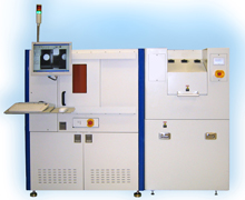
NWR launches automated, higher-throughput LED wafer-scribing systems
New Wave Research Inc (NWR) of Fremont, CA, USA has launched the AccuScribe 2112 and 2150 high-speed LED wafer-scribing systems, which have a throughput of 12-14 wafers per hour (compared to 10 wafers per hour for their predecessor, the AccuScribe AS2000FX, launched in July 2006) as well as a rugged and customizable platform optimized for demanding 24/7 production-line environments.
The platform provides four-inch wafer support capability and is easily customized. Backside alignment ( a feature unique to AccuScribe, it is claimed ) enables scribing from the backside of wafers when opaque materials preclude topside alignment and scribing.
Features for enhancing work efficiency include a highly accurate, repeatable and reliable X-Y stage, user-selectable energy output with stability feedback loop, and advanced debris removal system.
High-speed performance is achieved via high-efficiency, high-stability, ultraviolet diode-pumped solid-state (DPSS) laser technology and NWR’s optical and image-processing technologies. Performance-enhancing features include a patented wafer edge detection system that enables scribing of partial or broken wafers, increasing yields.
The semi-automated 2112 features automated alignment, positioning, and focus. The fully automated 2150 adds automated loading/unloading of wafers from/to cassettes.
 “Automation will significantly reduce man hours, minimize human error and boost overall process uniformity,” says product manager Pete Manautou. “Moreover, there's very little operator training or specialized skill necessary - users just program-in their scribing parameters.”
Picture: The fully automated 2150 adds automated loading/unloading of wafers from/to cassettes.
*ESI acquiring New Wave Research
On 5 July, Electro Scientific Industries Inc of Portland, OR, USA agreed to acquire New Wave Research for $36m (roughly equal to NWR’s annual revenue). The acquisition was expected to close within 30 days (subject to shareholder approval).
Founded in 1944, ESI supplies photonics and laser systems for precision fine-tuning of microelectronics device features in high-volume manufacturing environments.
“ESI’s acquisition of NWR accelerates our mutual growth strategies by leveraging our combined core competencies into adjacent markets,” says ESI’s president and CEO Nick Konidaris.
Founded in 1990, NWR has 150 staff and provides laser-based applications, with an extensive installed base and direct presence in the USA, Europe, and Asia. In the semiconductor market, its products are used for sapphire wafer scribing, flat-panel display repair and semiconductor failure analysis. NWR also produces laser ablation and other tools for industrial and scientific applications, as well as laser-micromachining tools for drilling, etching, and scribing a wide variety of materials.
“NWR will give us entry into the sapphire wafer scribing market through their Accuscribe systems,” says Konidaris. “Together our strong research and development talent pool will provide us with centers of excellence in Portland, Montana, and Silicon Valley to help accelerate the development of new tools for both companies.”
ESI will enhance NWR’s products by providing scientific, engineering, and system-design capabilities, says NWR’s CEO and co-founder Pei Hsien Fang. “This alliance will also greatly benefit our customers by giving them access to a larger range of cutting-edge products in addition to an expanded support network.”
Pei Hsien Fang will join ESI as VP, reporting to Konidaris in charge of the New Wave Research Division.
Visit NWR: http://www.new-wave.com
Visit ESI: http://www.esi.com
![]() ©2007 Juno Publishing and Media Solutions Ltd. All rights reserved. Semiconductor Today and the editorial material contained within it and related media is the copyright of Juno Publishing and Media Solutions Ltd. Reproduction in whole or part without permission from Juno Publishing and Media Solutions Ltd is forbidden. In most cases, permission will be granted, if the author, magazine and publisher are acknowledged.
©2007 Juno Publishing and Media Solutions Ltd. All rights reserved. Semiconductor Today and the editorial material contained within it and related media is the copyright of Juno Publishing and Media Solutions Ltd. Reproduction in whole or part without permission from Juno Publishing and Media Solutions Ltd is forbidden. In most cases, permission will be granted, if the author, magazine and publisher are acknowledged.
Disclaimer: Material published within Semiconductor Today and related media does not necessarily reflect the views of the publisher or staff. Juno Publishing and Media Solutions Ltd and its staff accept no responsibility for opinions expressed, editorial errors and damage/injury to property or persons as a result of material published.
Semiconductor Today, Juno Publishing and Media Solutions Ltd, Suite no. 133, 20 Winchcombe Street, Cheltenham, GL52 2LY, UK
Web site by No Name No Slogan ![]()