| Home | About Us | Contribute | Bookstore | Advertising | Subscribe for Free NOW! |
| News Archive | Features | Events | Recruitment | Directory |
New MEMS White Paper
Download the latest Logitech white paper and learn more about MEMS processing technology and techniques

| FREE subscription |
| Subscribe for free to receive each issue of Semiconductor Today magazine and weekly news brief. |
News
20 July 2007
GaN-based LEDs the main consumer of nitride materials
With an annual volume of more than 5 million 2”-equivalent substrates, gallium nitride-based green, blue and white LEDs represent the main consumer of nitride substrates, targeting a $3.5bn market at the device level, according to the report 'New Perspectives for Nitride Materials and Devices' from Yole Développement (also available through Research and Markets). The current split shows that silicon carbide (SiC) substrates account for about 10% of total production, with sapphire accounting for the rest.
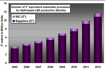
In 2006, the sapphire material market just exceeded the $150m mark, reckons Yole. The market for LEDs is now tending towards an equilibrium: two thirds of LEDs are manufactured on 2” substrates; one third are manufactured on 3” substrates (while Japan’s Showa Denko earlier this year started production of LEDs on 4” sapphire substrates).
SiC is also entering the 4” production stage at Cree Inc of Durham, NC, USA. However, it cannot be considered as a real open market, says the report (since Cree manufactures not only SiC substrates but also LEDs based on them).
Yole reckons that the nitride substrate market can be seen as being partially unstable, because of the rapid emergence of new substrates for GaN epitaxy. GaN-on-silicon, GaN-on-ZnO, GaN-on-germanium, GaN-on-glass, GaN-on-AlN and composite substrates like GaN-on-diamond or Picogiga’s GaN-on-SopSiC are now all pursuing the same goal: the best compromise between GaN quality, large substrate diameter, low bowing, high thermal conductivity, a controlled TCE (thermal coefficient of expansion) and, of course, low-cost. The main target is a 6” substrate, which is now available off-the-shelf from select companies. This is opening new doors to higher LED productivity for the huge solid-state lighting (SSL) general illumination market, says Yole.
In the RF market, GaN high-electron-mobility transistors (HEMTs) are now ready to challenge Si LDMOS and GaAs pHEMT in the telecom base-station market (3G, 4G, WiMAX, etc). With devices reaching a saturated power output (Psat) of 174W at 6GHz under 48V polarization, GaN technology can now be implemented both in the 2 million deployed mobile phone base-stations and in the coming WiMAX network infrastructure. Yole forecasts a market of 10,000 4”-diameter epiwafers in the very near future.
With GaN (like SiC) being a wide-bandgap material that allows high breakdown voltages, the road to power electronics applications is wide open, says Yole. However, GaN growth is based on a hetero-epitaxial process, often with an AlN nucleation layer, forcing devices to be designed laterally. Since lateral devices are limited in terms of breakdown voltage compared to vertical devices, they can rapidly become bulky in the high-power-density range.
This situation therefore involves a subtle trade-off between the substrate diameter, power density, chip size and device cost. But in other terms, GaN power devices on sapphire, silicon or composite substrates can compete with SiC from a cost point of view by using larger (4”) substrates to compensate for the bigger chip size that is required for a given power density, concludes the report.
Visit Yole: http://www.yole.fr/pagesAn/products/pdf/gan.pdf
Visit Research and Markets:
![]() ©2007 Juno Publishing and Media Solutions Ltd. All rights reserved. Semiconductor Today and the editorial material contained within it and related media is the copyright of Juno Publishing and Media Solutions Ltd. Reproduction in whole or part without permission from Juno Publishing and Media Solutions Ltd is forbidden. In most cases, permission will be granted, if the author, magazine and publisher are acknowledged.
©2007 Juno Publishing and Media Solutions Ltd. All rights reserved. Semiconductor Today and the editorial material contained within it and related media is the copyright of Juno Publishing and Media Solutions Ltd. Reproduction in whole or part without permission from Juno Publishing and Media Solutions Ltd is forbidden. In most cases, permission will be granted, if the author, magazine and publisher are acknowledged.
Disclaimer: Material published within Semiconductor Today and related media does not necessarily reflect the views of the publisher or staff. Juno Publishing and Media Solutions Ltd and its staff accept no responsibility for opinions expressed, editorial errors and damage/injury to property or persons as a result of material published.
Semiconductor Today, Juno Publishing and Media Solutions Ltd, Suite no. 133, 20 Winchcombe Street, Cheltenham, GL52 2LY, UK
Web site by No Name No Slogan ![]()