| Home | About Us | Contribute | Bookstore | Advertising | Subscribe for Free NOW! |
| News Archive | Features | Events | Recruitment | Directory |
New MEMS White Paper
Download the latest Logitech white paper and learn more about MEMS processing technology and techniques
| FREE subscription |
| Subscribe for free to receive each issue of Semiconductor Today magazine and weekly news brief. |
News
4 May 2007
UCSB achieves high-efficiency non-polar GaN LEDs at improved output power
The research group at the University of Califormia, Santa Barbara (UCSB) led by blue LED pioneer Shuji Nakamura and Steve DenBaars has fabricated improved MOCVD-grown non-polar m-plane GaN LEDs with a thick, six-period InGaN multi-quantum-well (MQW) active region that have record output power and external quantum efficiency at the peak blue-violet emission wavelength of 402nm (Kwang-Choong Kim et al, physica status solidi - Rapid Research Letters, Vol 1, issue 3 (May), p125 ).
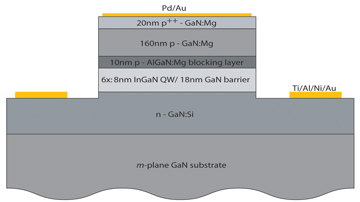
Non-polar GaN should yield higher-efficiency LEDs than conventional polar c-plane GaN material. But p reviously the conversion efficiency and output power of non-polar GaN LEDs have been lower due to the high density of extended defects (such as threading dislocations and basal stacking faults) in non-polar GaN material grown heteroepitaxially on foreign substrate types such as r-plane sapphire or m-plane silicon carbide.
However, in mid-December, the researchers reported record external quantum efficiency of 41% and output power of 25mW for a non-polar GaN LED with a standard chip size (300µm x 300µm) and pulsed operating current (20mA). Now, also at a pulsed driving current of 20mA, the latest LED’s output power is 28mW and the external quantum efficiency is 45.4%. But more significantly, with increasing drive current the output power increases almost linearly up to 210mW at 160mA and, at a high drive current of 200mA, is as much as 250mW (showing hardly any signs of saturation, in contrast to conventional polar c-plane GaN LEDs). External quantum efficiency is still a high 41% at 200mA.
 The latest improvements are due partly to using low-extended-defect free-standing m-plane GaN substrates sliced from c-plane bulk GaN crystals, which recently became commercially available, manufactured by the Optoelectronics Laboratory of Japan’s Mitsubishi Chemical Corp using hydride vapor phase epitaxy (HVPE).
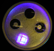
Picture: UCSB's high-efficiency non-polar GaN LED
Also, as well as using a conventional 300µm x 300µm chip design with an unoptimized indium tin oxide (ITO) p-type contact and a U-shaped Ti/Al/Au n-type contact and standard processing techniques , the LED chips were diced and packaged using standard die and wire bonding techniques and then molded with epoxy. So external efficiencies at high power could be improved further by using optimized ITO p-contacts and more advanced fabrication techniques.
However, in a commentary article in the same issue of physica status solidi, Ulrich Schwarz of the Institut für Experimentelle und Angewandte Physik, Universität Regensburg and Michael Kneissl of the Institut für Festkörperphysik, Technische Universität Berlin in Germany say that one of the greatest challenges is the development of large-area substrates und inexpensive non-polar GaN structures. Also, an extension of the 402nm emission wavelength to the blue and green spectral region also needs to be considered. In addition, the lifetime of the LEDs must be established.
Due to the current high cost of non-polar GaN substrates, Schwarz and Kneissl expect the initial applications of non-polar GaN to be not blue and white LEDs but laser diodes (e.g. for micro-projector displays in mobile phones or for high-resolution home theatre projectors.
The research is funded by the Solid State Lighting and Display Center (SSLDC) at UCSB and the Exploratory Research for Advanced Technology (ERATO) program of the Japan Science & Technology Agency.
See related item:
Record efficiency non-polar and semipolar GaN LEDs
Visit UCSB: http://www.engineering.ucsb.edu
Download abstract at:
http://www3.interscience.wiley.com/cgi-bin/abstract/114209832/ABSTRACT
![]() ©2007 Juno Publishing and Media Solutions Ltd. All rights reserved. Semiconductor Today and the editorial material contained within it and related media is the copyright of Juno Publishing and Media Solutions Ltd. Reproduction in whole or part without permission from Juno Publishing and Media Solutions Ltd is forbidden. In most cases, permission will be granted, if the author, magazine and publisher are acknowledged.
©2007 Juno Publishing and Media Solutions Ltd. All rights reserved. Semiconductor Today and the editorial material contained within it and related media is the copyright of Juno Publishing and Media Solutions Ltd. Reproduction in whole or part without permission from Juno Publishing and Media Solutions Ltd is forbidden. In most cases, permission will be granted, if the author, magazine and publisher are acknowledged.
Disclaimer: Material published within Semiconductor Today and related media does not necessarily reflect the views of the publisher or staff. Juno Publishing and Media Solutions Ltd and its staff accept no responsibility for opinions expressed, editorial errors and damage/injury to property or persons as a result of material published.
Semiconductor Today, Juno Publishing and Media Solutions Ltd, Suite no. 133, 20 Winchcombe Street, Cheltenham, GL52 2LY, UK
Web site by No Name No Slogan ![]()