| Home | About Us | Contribute | Bookstore | Advertising | Subscribe for Free NOW! |
| News Archive | Features | Events | Recruitment | Directory |
New MEMS White Paper
Download the latest Logitech white paper and learn more about MEMS processing technology and techniques
| FREE subscription |
| Subscribe for free to receive each issue of Semiconductor Today magazine and weekly news brief. |
News
1 May 2007
Institute of Semiconductor Technology, University of Braunschweig orders CV wafer profiler from WEP
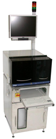
Germany’s Institute of Semiconductor Technology, part of the University of Braunschweig, has ordered a CVP21 electrochemical CV wafer profiler from WEP (Wolff für Elektronik- und Programmentwicklungen) of Furtwangen im Schwarzwald, Germany.
The Institute undertakes research into a broad range of semiconductor materials, including silicon, germanium, silicon carbide, arsenides, phosphides, antimonides, nitrides, and zinc oxide.
The CVP21 measures doping profiles in semiconductor layers by Electrochemical Capacitance Voltage Profiling (ECV Profiling, CV Profiling), and according to WEP it can be used directly after epitaxial growth without the need for a sample preparation. Measurements can be made on wafer samples of up to 8” in diameter, but only a local spot of 1mm² or 10mm² is etched. The CV wafer profiler can check:
- Doping of layers
- Doping gradients
- Quality of layer interfaces (also in hetero-structures)
 WEP adds that the CVP21’s handling of water-based electrolytes is automated; the measurement is completely computer controlled. When the measurement process is complete, the local etch spot is washed and dried automatically with nitrogen.
The CVP21 has a footprint of 60(W) x 80(D) x 195(H)cm, and is also available as a table-top unit.
As well as its CVP21 wafer profiler, WEP offers process control systems and software.
Picture: CVP21 electrochemical CV wafer profiler from WEP
See related item:
University begins operating newly installed Thomas Swan CCS system for GaN/ZnO production
Visit WEP: http://www.wepcontrol.com
Visit IHT: http://www.iht.tu-bs.de
![]() ©2007 Juno Publishing and Media Solutions Ltd. All rights reserved. Semiconductor Today and the editorial material contained within it and related media is the copyright of Juno Publishing and Media Solutions Ltd. Reproduction in whole or part without permission from Juno Publishing and Media Solutions Ltd is forbidden. In most cases, permission will be granted, if the author, magazine and publisher are acknowledged.
©2007 Juno Publishing and Media Solutions Ltd. All rights reserved. Semiconductor Today and the editorial material contained within it and related media is the copyright of Juno Publishing and Media Solutions Ltd. Reproduction in whole or part without permission from Juno Publishing and Media Solutions Ltd is forbidden. In most cases, permission will be granted, if the author, magazine and publisher are acknowledged.
Disclaimer: Material published within Semiconductor Today and related media does not necessarily reflect the views of the publisher or staff. Juno Publishing and Media Solutions Ltd and its staff accept no responsibility for opinions expressed, editorial errors and damage/injury to property or persons as a result of material published.
Semiconductor Today, Juno Publishing and Media Solutions Ltd, Suite no. 133, 20 Winchcombe Street, Cheltenham, GL52 2LY, UK
Web site by No Name No Slogan ![]()