
| Home | About Us | Contribute | Bookstore | Advertising | Subscribe for Free NOW! |
| News Archive | Features | Events | Recruitment | Directory |
CMP PROCESSING
Learn more about R&D chemical mechanical polishing by requesting our FREE informational CD.

| FREE subscription |
| Subscribe for free to receive each issue of Semiconductor Today magazine and weekly news brief. |
News
8 November 2007
Aixtron buys Nanometrics VerteX PL mapping system
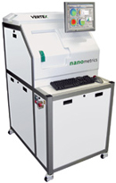 Metrology equipment manufacturer Nanometrics Inc of Milpitas, CA, USA says that deposition equipment maker Aixtron AG of Aachen, Germany has bought a VerteX photoluminescence (PL) mapping system, to be installed at its demonstration facility in Aachen, Germany during fourth-quarter 2007. The system will be used to determine material composition, measure layer thickness and improve the wafer uniformity performance of its equipment.
“The VerteX system will be a tremendous asset to our demonstration facility,” says professor Michael Heuken, VP corporate R&D at Aixtron. “Not only will we be able to monitor the performance and accuracy of our equipment, but our customers will get quantifiable data from our tool as well,” he adds. “Our installation of the VerteX system will give our facility the most advanced production PL mapping capability on the market today, which is required to demonstrate the advantages of our recently introduced reactors with larger production capacity.”
The VerteX will replace Aixtron’s current PL mapping tool, a Nanometrics’ RPM2000, in order to obtain greater execution for its deposition systems and processes. “This purchase of our VerteX system marks another milestone in our long-term relationship with Aixtron,” says Tom Ryan, Nanometrics' business unit manager, Materials Characterization. The collaboration with Aixtron will give great insight into future technology, which will help Nanometrics to advance its PL mapping technology, he adds.
See related item:
Nanometrics introduces VerteX; plans R&D expansion at York facility
Search: Aixtron
Visit: www.nanometrics.com
Visit: www.aixtron.com![]()
![]() ©2007 Juno Publishing and Media Solutions Ltd. All rights reserved. Semiconductor Today and the editorial material contained within it and related media is the copyright of Juno Publishing and Media Solutions Ltd. Reproduction in whole or part without permission from Juno Publishing and Media Solutions Ltd is forbidden. In most cases, permission will be granted, if the author, magazine and publisher are acknowledged.
©2007 Juno Publishing and Media Solutions Ltd. All rights reserved. Semiconductor Today and the editorial material contained within it and related media is the copyright of Juno Publishing and Media Solutions Ltd. Reproduction in whole or part without permission from Juno Publishing and Media Solutions Ltd is forbidden. In most cases, permission will be granted, if the author, magazine and publisher are acknowledged.
Disclaimer: Material published within Semiconductor Today and related media does not necessarily reflect the views of the publisher or staff. Juno Publishing and Media Solutions Ltd and its staff accept no responsibility for opinions expressed, editorial errors and damage/injury to property or persons as a result of material published.
Semiconductor Today, Juno Publishing and Media Solutions Ltd, Suite no. 133, 20 Winchcombe Street, Cheltenham, GL52 2LY, UK
Web site by No Name No Slogan ![]()