| Home | About Us | Contribute | Bookstore | Advertising | Subscribe for Free NOW! |
| News Archive | Features | Events | Recruitment | Directory |
| FREE subscription |
| Subscribe for free to receive each issue of Semiconductor Today magazine and weekly news brief. |
News
12 October 2006
TDI demos technology for GaN and AlGaN QWs and Superlattices
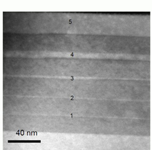
Technologies and Devices International Inc of Silver Spring, MD, USA says it has fabricated gallium nitride quantum well (QW) structures using novel hydride vapor phase epitaxy (HVPE).
HVPE is TDI’s core technology, which it uses to produce a variety of GaN-based epitaxial products. “TDI has perfected the growth of very thick GaN layers, which is typical of the HVPE process, along with very thin layers and multi-layer structures, in the same epitaxial process,” says Vladimir Dmitriev, president and CEO.
“TDI engineers and scientists have successfully developed a novel HVPE growth machine and process which allows us to reduce the materials deposition rate by more than two orders of magnitude and control the growth of GaN, AlN, and AlGaN layers to a thickness of about 1nm,” Dmitriev added.
Professor Subhash Mahajan, his student Fanyu Meng and post-doctoral fellow Ranjan Datta at Arizona State University have characterized GaN single and multiple quantum well structures fabricated at TDI. “HVPE is a well-known method to fabricate thick GaN layers. We never expected this technology to produce nanometer-thick GaN layers and multi-layer structures,” they comment. Their transmission electron microscopy measurements on recent TDI samples confirm that this is indeed achieved, they say. “This is definitely the first HVPE-grown AlGaN/GaN structure that clearly shows a quantum well signature in photoluminescent characterization,” adds Professor Michael Reshchikov of Virginia Commonwealth University.
“This proprietary HVPE process opens up a completely new path for the formation of low-defect substrate materials and device structures,” says Dmitriev. Quantum well structures are the key elements for devices including high-brightness LEDs and laser diodes. Multi-layer structures with nanometer-scale layers are important to reduce defects and control strain in GaN-based materials, to improve doping, and to open new device possibilities.
TDI will report the results on HVPE grown GaN-based quantum well structures at the International Workshop on Nitride Semiconductors 2006 (22-27 October) in Kyoto, Japan, and feature the MQW epitaxial wafers at the workshop's exhibition.
With continued support for the developments from the US Department of Energy (DoE) and Defense Advanced Research Project Agency (DARPA), TDI plans to release epitaxial products based on HVPE grown superlattice structures and quantum wells in early 2007.
Visit: http://www.tdii.com
![]() ©2006 Juno Publishing and Media Solutions Ltd. All rights reserved. Semiconductor Today and the editorial material contained within it and related media is the copyright of Juno Publishing and Media Solutions Ltd. Reproduction in whole or part without permission from Juno Publishing and Media Solutions Ltd is forbidden. In most cases, permission will be granted, if the author, magazine and publisher are acknowledged.
©2006 Juno Publishing and Media Solutions Ltd. All rights reserved. Semiconductor Today and the editorial material contained within it and related media is the copyright of Juno Publishing and Media Solutions Ltd. Reproduction in whole or part without permission from Juno Publishing and Media Solutions Ltd is forbidden. In most cases, permission will be granted, if the author, magazine and publisher are acknowledged.
Disclaimer: Material published within Semiconductor Today and related media does not necessarily reflect the views of the publisher or staff. Juno Publishing and Media Solutions Ltd and its staff accept no responsibility for opinions expressed, editorial errors and damage/injury to property or persons as a result of material published.
Semiconductor Today, Juno Publishing and Media Solutions Ltd, Suite no. 133, 20 Winchcombe Street, Cheltenham, GL52 2LY, UK
Web site by No Name No Slogan ![]()